

Programmable memory cell in an integrated circuit chip
- Summary
- Abstract
- Description
- Claims
- Application Information
AI Technical Summary
Benefits of technology
Problems solved by technology
Method used
Image

Examples
Embodiment Construction
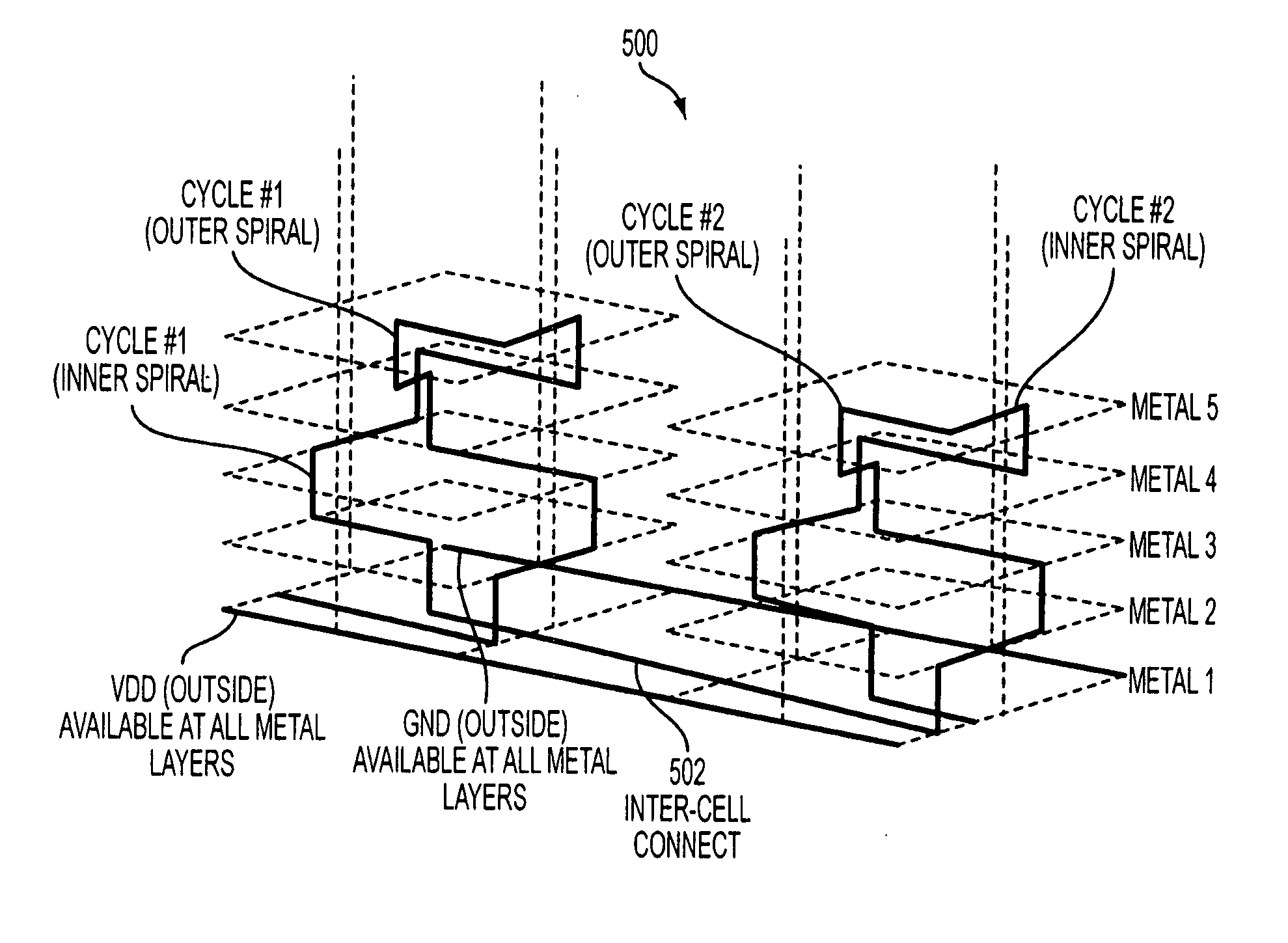
[0049] The preferred embodiment of the present invention will now be discussed in detail. While specific features, configurations and arrangements are discussed, it should be understood that this is done for illustration purposes only. A person skilled in the relevant art will recognize that other steps, configurations and arrangements or devices may be used to achieve the features of the invention without departing from the spirit and scope thereof. Indeed, for the sake of brevity, conventional electronics, manufacturing of semiconductor devices, and other functional aspects of the method / apparatus (and components of the individual operating components of the apparatus) may not be described in detail herein.
[0050] The terms chip, integrated circuit, monolithic device, semiconductor device, and microelectronic device are often used interchangeably in this field. The present invention is applicable to all the above as they are generally understood in the field.
[0051] The material c...
PUM
 Abstract
Description
Claims
Application Information