Organic EL light-emitting device and production method thereof

a light-emitting device and organic technology, applied in the field of organic electroluminescence, can solve problems such as crosstalk between adjacent pixels of the same color, and achieve the effect of preventing crosstalk between adjacent pixels

Inactive Publication Date: 2007-06-14
CANON KK
View PDF8 Cites 30 Cited by
  • Summary
  • Abstract
  • Description
  • Claims
  • Application Information

AI Technical Summary

Benefits of technology

[0010] It is, therefore, an object of the present invention to provide a method of producing an organic EL light-emitting device, which is capable of preventing crosstalk between adjacent pixels of the same color.
[0013] According to the present invention, an organic EL material is applied by the nozzle printing in a state in which low banks (banks of a row direction) are formed in a direction which intersects the scanning direction, whereby crosstalk between adjacent pixels of the same color can be prevented.

Problems solved by technology

Accordingly, there is posed the problem of crosstalk between adjacent pixels of the same color.

Method used


Image

  • Organic EL light-emitting device and production method thereof
  • Organic EL light-emitting device and production method thereof
  • Organic EL light-emitting device and production method thereof

Examples


embodiment 1

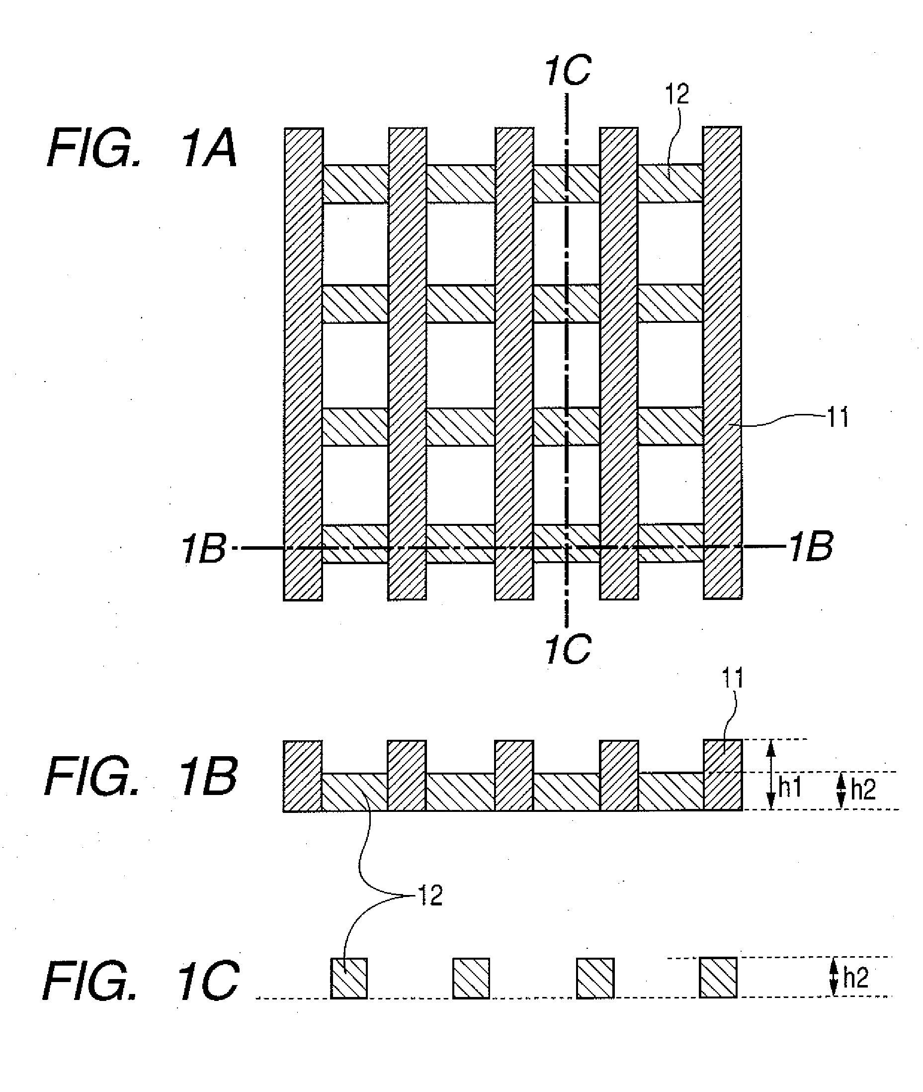
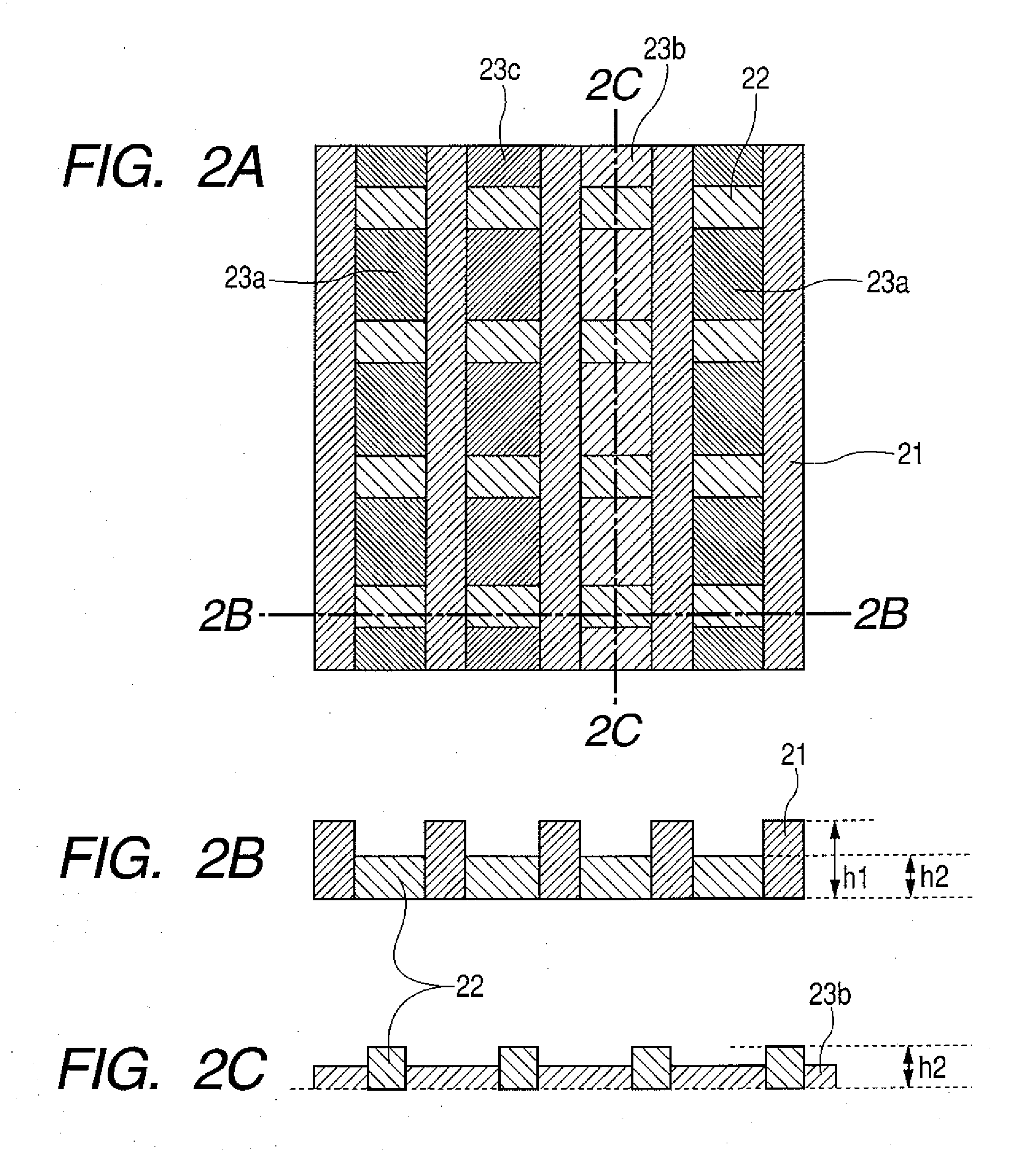
[0034]FIGS. 1A, 1B, and 1C are schematic views showing banks of an organic EL light-emitting device according to Embodiment 1 of the present invention. FIGS. 2A, 2B, and 2C are schematic views showing a state in which an organic compound layer is provided in each of areas defined by the banks of the organic EL light-emitting device, according to Embodiment 1 of the present invention. FIGS. 1A and 2A are plan views, and FIGS. 1B, 1C, 2B and 2C are cross-sectional views. In the organic EL light-emitting device of the present invention, electrodes are provided under the organic compound layer (back side of the drawing) and on the organic compound layer (front side of the drawing). However, in FIGS. 1A to 1C and FIGS. 2A to 2C, the devices are represented schematically with the electrodes being omitted for convenience of presentation. The organic EL light-emitting device of the present invention may be of the so-called passive matrix type in which striped electrodes intersect each other...

embodiment 2

[0043]FIGS. 3A, 3B, and 3C are schematic views showing banks of an organic EL light-emitting device according to Embodiment 2 of the present invention. FIGS. 4A, 4B, and 4C are schematic views showing a state in which an organic compound layer is provided in each of areas defined by the banks of the organic EL light-emitting device, according to Embodiment 2 of the present invention. FIGS. 3A and 4A are plan views, and FIGS. 3B, 3C, 4B and 4C are cross-sectional views. In the organic EL light-emitting device of the present invention, electrodes are provided under the organic compound layer (back side of the drawing) and on the organic compound layer (front side of the drawing). However, in FIGS. 3A to 3C and FIGS. 4A to 4C, the devices are represented schematically with the electrodes being omitted for convenience of presentation.

[0044] In FIGS. 3A, 3B, and 3C, reference numeral 31 denotes bank portions of a column direction, and reference numeral 32 denotes bank portions of a row ...

example 1

[0053] In the present example, an organic EL light-emitting device according to Embodiment 1 was produced.

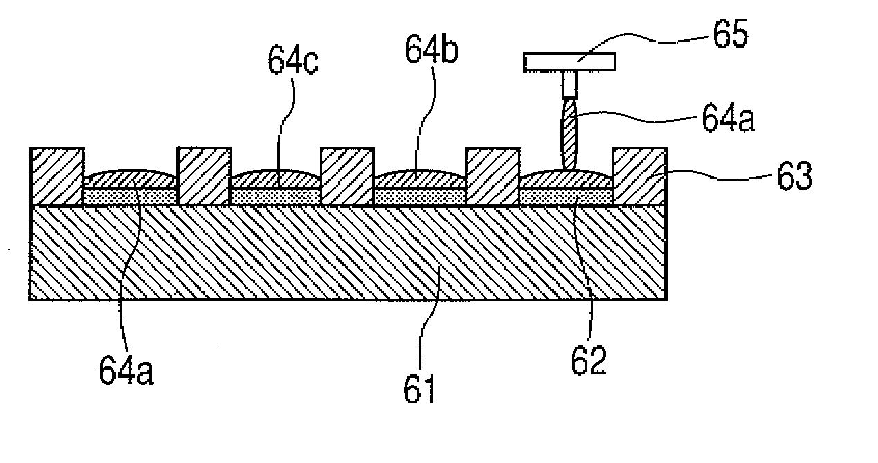
[0054] First, a method of producing an organic EL light-emitting device using the conventional nozzle printing is described below with reference to FIG. 6 (cross sectional view) and FIG. 7 (plan view), each of which illustrates organic EL light-emitting portions of the organic EL light-emitting device.

[0055] In the conventional nozzle printing process, organic EL layers, such as a hole injection layer and a light-emitting layer (red 64a, blue 64b, and green 64c) are formed between banks 63 by coating using a nozzle 65. At this time, the technique of continuously dropping a liquid ink (organic EL material, for example, 64) is adopted, so that the problem associated with the use of the conventional ink jet system such as shown in FIG. 8 that droplets of ink (organic EL material, for example, 84) go across the banks to be mixed into adjacent pixels is resolved.

[0056] However, as...


PUM


Abstract

There is provided a method of producing an organic EL light-emitting device which enables prevention of crosstalk between adjacent pixels of the same color. Provided is a method of producing an organic EL light-emitting device which has banks provided in a row direction and in a column direction, and a plurality of organic EL light-emitting portions isolated from each other by the banks. The method includes the steps of forming banks such that a height of a bank portion of a row direction and a height of a bank portion of a column direction are different from each other; and applying an organic EL material in a continuous manner along the bank portion which is higher of the bank portion of the row direction and the bank portion of the column direction, between the banks of the higher bank portion.

Description

BACKGROUND OF THE INVENTION [0001] 1. Field of the Invention [0002] The present invention relates to an organic electroluminescence (hereinafter, simply referred to as “EL”) light-emitting device utilizing EL of an organic compound material which emits light when current is injected therein, and a production method thereof. More particularly, the present invention relates to an organic EL light-emitting device having banks for isolating pixels, and a production method thereof. [0003] 2. Description of the Related Art [0004] In the production of the organic EL light-emitting device, which is promising for a large-area display, an organic EL light-emitting material has been applied to a large-size substrate in an attempt to reduce the production cost. [0005] Japanese Patent Application Laid-Open No. H10-153967 discloses a method of fabricating a light-emitting device using an inkjet system, which is a typical method for applying such a material. The method is described below. [0006] A...

Claims


Application Information

Patent Timeline
Patent Type & Authority Applications(United States)
IPC IPC(8): H01J19/42H01J1/88H01K1/18
CPCH01L27/3211H01L27/3246H01L27/3283H10K59/35H10K59/122H10K59/173
Inventor HASHIMOTO, MORIMINAKANISHI, MASAHIROMIMURA, TOSHIHIKO
Owner CANON KK
Why Eureka
Try Eureka