
Partial-via-first dual-damascene process with tri-layer resist approach

a dual-damascene and resist technology, applied in the direction of basic electric elements, semiconductor/solid-state device manufacturing, electric apparatus, etc., can solve the problems of photoresist poisoning, difficult to adequately control the etch process, etc., to avoid ashing damage, improve critical-dimension control, and avoid the effect of ashing damag

Inactive Publication Date: 2007-06-14
TAIWAN SEMICON MFG CO LTD
View PDF6 Cites 26 Cited by
  • Summary
  • Abstract
  • Description
  • Claims
  • Application Information

AI Technical Summary

Benefits of technology

[0005] Embodiments of the present invention include a partial-via-first dual-damascene method using a tri-layer resist process to improve critical-dimension control for via holes and trench, avoid ashing damage, and provide a wide wet strip window in patterning via holes without extra process flow and production costs.

Problems solved by technology

Some low-k dielectric materials are porous, and it is difficult to adequately control the etch process, particularly in the dual-damascene structure and process.
Photoresist poisoning, however, tends to be a problem in the full-via-first dual-damascene process because of the subsequent photoresist exposed to amines generated during the previous etch process.
The other approach of using a metal hardmask has been applied to the trench-first dual-damascene process for preventing plasma damages in photoresist stripping, but via misalignment and metallic polymer removal are the disadvantages of this approach.

Method used


Image

  • Partial-via-first dual-damascene process with tri-layer resist approach
  • Partial-via-first dual-damascene process with tri-layer resist approach
  • Partial-via-first dual-damascene process with tri-layer resist approach

Examples


Embodiment Construction

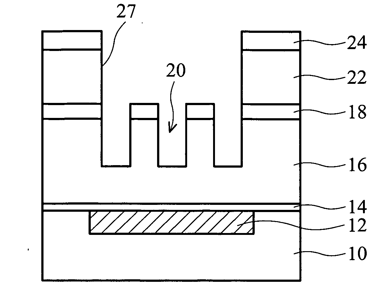
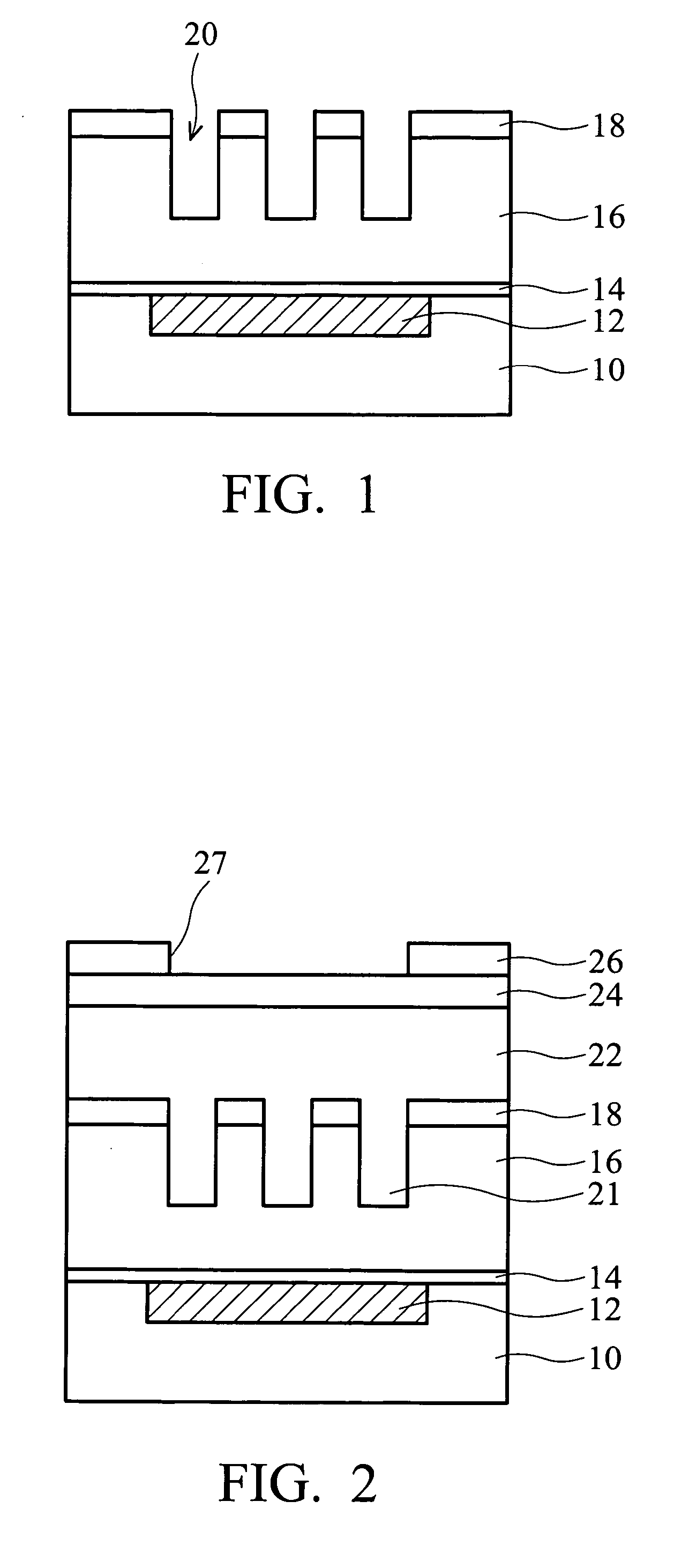
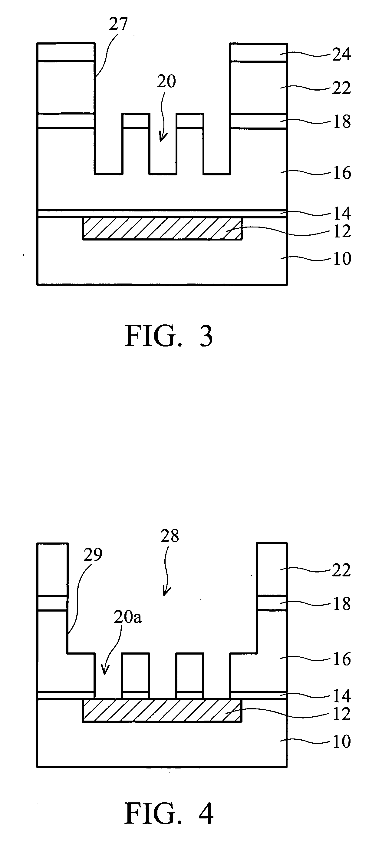
[0010] Embodiments of the present invention provide a novel dual-damascene process, which overcomes the aforementioned problems of the prior art through the use of a tri-layer resist process and a metal hard mask process. Particularly, a partial-via-first dual-damascene method with a tri-layer resist process is employed to improve critical-dimension (CD) control for via holes and trenches, avoid ashing damage, and provide a wide wet strip window in patterning via holes without extra process flow and production costs. Compared with the conventional full-via-first method, the term “partial-via-first” as used throughout this disclosure refers to a dual-damascene method in which an initial via hole is patterned first through partial thickness of a dielectric layer by reducing the depth of the initial via etch, and then a real via hole is patterned in the lower portion of the dielectric layer and a trench is patterned in the upper portion of the dielectric layer.

[0011] Reference will no...


PUM


Abstract

A partial-via-first dual-damascene method using a tri-layer resist method forms a first via hole through partial thickness of a dielectric layer, and forms a tri-layer resist structure on the dielectric layer to fill the first via hole with the bottom photoresist layer. A dry development process is performed to transfer a first opening on the top photoresist layer to the middle layer and the bottom photoresist layer, and expose the first via hole again, and remove the top photoresist layer. A dry etching process is then performed to form a second via hole under the first via hole and a trench over the second via hole. Finally a wet striping process is used to remove the remainder of the photoresist layer.

Description

TECHNICAL FIELD [0001] The present invention relates to the fabrication of structures for integrated circuit devices, and particularly to a partial-via-first dual-damascene process using a tri-layer resist approach. BACKGROUND [0002] Dual-damascene interconnect features are advantageously used to provide planarized interconnect structures that afford the use of multiple interconnect layers and therefore increase levels of device integration. There is a trend in the semiconductor industry towards the use of low-dielectric constant (low-k) dielectric materials, particularly used in conjunction with copper conductive lines, to reduce the RC time delay of the conductive lines. Some low-k dielectric materials are porous, and it is difficult to adequately control the etch process, particularly in the dual-damascene structure and process. [0003] Dual-damascene methods include either a “via-first” patterning methods in which via holes are first patterned in the insulating layer through the ...

Claims


Application Information

Patent Timeline
Patent Type & Authority Applications(United States)
IPC IPC(8): H01L21/4763
CPCH01L21/76808H01L21/7681H01L21/76813
Inventor LI, TSAI-CHUNWU, TSANG-JIUHOUYANG, HUI
Owner TAIWAN SEMICON MFG CO LTD
Learn More