Run to run control process for controlling critical dimensions

a control process and critical dimension technology, applied in semiconductor/solid-state device testing/measurement, measurement devices, instruments, etc., can solve problems such as speed performance and power consumption of circuits, loss of linewidth control including the entire loss, contamination with airborne particles and air bubbles, etc., to achieve substantially improved control of critical dimension uniformity, improve manufacturability and control

Inactive Publication Date: 2007-03-13
LONE STAR SILICON INNOVATIONS LLC
View PDF11 Cites 19 Cited by
  • Summary
  • Abstract
  • Description
  • Claims
  • Application Information

AI Technical Summary

Benefits of technology

[0018]Many advantages are achieved by the described process control method. One advantage is that the control of critical dimension uniformity is substantially improved by the described process. It is also highly advantageous that the described method improves manufacturability as well as control.

Problems solved by technology

Poor adhesion can cause a loss of linewidth control including the entire loss of pattern elements in extreme cases.
Contamination with airborne particles and air bubbles can occur during the coating step.
The critical dimensions of polysilicon gates affect many operating parameters of integrated circuits, but fundamentally the greatest considerations of critical dimensions is speed performance and power consumption of a circuit.
Too small a polysilicon gate critical dimension, however, results in unacceptably high power consumption and parasitic currents in the transistor.
Unfortunately, the critical dimensions resulting from conventional manufacturing methods are rarely optimum, resulting in reduced yield of high performance circuits.
Furthermore, the conventional process is very wasteful when process conditions are substandard.

Method used


Image

  • Run to run control process for controlling critical dimensions
  • Run to run control process for controlling critical dimensions
  • Run to run control process for controlling critical dimensions

Examples


Embodiment Construction

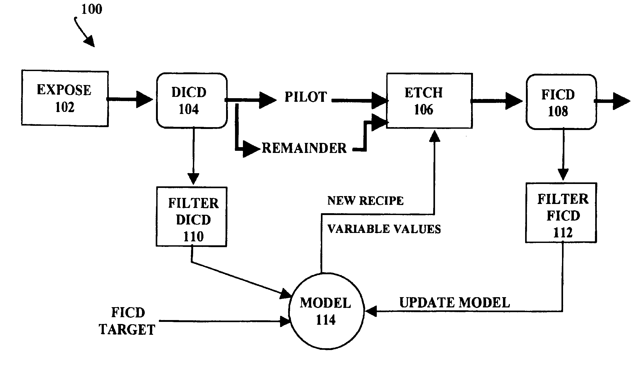
[0023]Referring to FIG. 1, a flow chart illustrates a control method for controlling critical dimensions in a semiconductor fabrication process 100 by adjusting the fabrication parameters or “recipe” for a photoresist etch step 106 previous to a polysilicon gate etch step in the fabrication process 100. In particular, the critical dimensions are controlled using photoresist etch time as a control variable to drive the critical dimensions to a target value.

[0024]In overview, the fabrication process 100 involves selection of one or more test wafers, called “pilot” wafers from an entire lot of wafers. The pilot wafers are tested to characterize the lot of wafers, processed through the photoresist etch step 106 using a nominal, average, or moving average processing recipe, and measured in a Final Inspection Critical Dimensions step 108. The results from the pilot lot tests are applied to update a process model 114 which is used to adjust the etch recipe for the remaining wafers in the l...


PUM


Abstract

It has been discovered that all causes of critical dimension variation, both known and unknown, are compensated by adjusting the time of photoresist etch. Accordingly, a control method employs a control system using photoresist etch time as a manipulated variable in either a feedforward or a feedback control configuration to control critical dimension variation during semiconductor fabrication. By controlling critical dimensions through the adjustment of photoresist etch time, many advantages are achieved including a reduced lot-to-lot variation, an increased yield, and increased speed of the fabricated circuits. In one embodiment these advantages are achieved for polysilicon gate critical dimension control in microprocessor circuits. Polysilicon gate linewidth variability is reduced using a control method using either feedforward and feedback or feedback alone. In some embodiments, feedback control is implemented for controlling critical dimensions using photoresist each time as a manipulated variable. In an alternative embodiment, critical dimensions are controlled using RF power as a manipulated variable. A run-to-run control technique is used to drive the critical dimensions of integrated circuits to a set specification. In a run-to-run control technique a wafer test or measurement is made and a process control recipe is adjusted based on the result of the test or measurement on a run-by-run basis. The run-to-run control technique is applied to drive the critical dimensions of a polysilicon gate structure to a target specification. The run-to-run control technique is applied to drive the critical dimensions in an integrated circuit to a defined specification using photoresist etch time as a manipulated variable.

Description

BACKGROUND OF THE INVENTION[0001]1. Field of the Invention[0002]The present invention relates to semiconductor fabrication methods. More precisely, the present invention relates to a control system used in semiconductor fabrication for controlling feature critical dimensions.[0003]2. Description of the Related Art[0004]Two aspects of feature sizes are controlled in a lithographic and etch process. The first aspect is a critical dimension, the absolute size of a feature, including linewidth, spacing or contact dimensions. The second aspect is the variation in feature size across the wafer surface as measured by steps of a wafer stepper. Linewidth and spacing measurements are regularly performed to determine the actual sizes of critical dimensions at each masking level of a process.[0005]Another aspect of linewidth control is that correct feature sizes are to be maintained across an entire wafer and also maintained from wafer to wafer. As a feature size is reduced, the tolerable error...

Claims


Application Information

Patent Timeline
Patent Type & Authority Patents(United States)
IPC IPC(8): H01L21/66H01L21/302
CPCH01L22/20
Inventor TOPRAC, ANTHONY JOHNDOWNEY, DOUGLAS JOHNGUPTA, SUBHASH
Owner LONE STAR SILICON INNOVATIONS LLC
Why Eureka
Try Eureka