Geometrically optimized spacer to improve device performance

Inactive Publication Date: 2006-07-06
TAIWAN SEMICON MFG CO LTD
View PDF5 Cites 10 Cited by
  • Summary
  • Abstract
  • Description
  • Claims
  • Application Information

AI Technical Summary

Benefits of technology

[0009] To achieve the foregoing and other objects, and in accordance with the purposes of the present invention, as embodied and broadly described herein, the present invention provides a CMOS device with trapezoid shaped spacers and a method for forming the same with improved critical dimension control and improved salicide formation.

Problems solved by technology

As MOSFET and CMOS device characteristic sizes are scaled below 0.1 microns including below 45 nm, the process window for wet and dry etching processes are increasingly difficult to control to achieve desired critical dimensions.
For example, in forming dielectric spacers, also referred to as sidewall spacers or main spacers, it is particularly difficult to control the width of the spacers, especially when subjected to subsequent self aligned silicide (salicide) formation processes.
As device sizes decrease below about 0.13 microns, both the deposition process and the etching process have extremely narrow process windows whereby dimensional variations undesirably alter critical dimensions (CD's) and electrical performance of the CMOS device.
Problems with theses geometrical configurations include the shortcomings that the width of L-shaped spacers are extremely difficult to control to achieve widths within design rule criteria, including device pitch considerations.
For example, the bottom portion of the L-shaped spacer is easily altered in etching processes, whereby a small (e.g., a few nanometers) variation in width overlying the SDE region results in a large percentage variation according to design rules, thereby detrimentally affecting device performance.
On the other hand, triangular shaped spacers, which do not have vertically disposed sidewalls, have the shortcoming that in a subsequent etching process, the exposed sidewalls of the spacers are exposed to the etching process, thereby undesirably altering the width of the triangular shaped spacer.

Method used


Image

  • Geometrically optimized spacer to improve device performance
  • Geometrically optimized spacer to improve device performance
  • Geometrically optimized spacer to improve device performance

Examples


Embodiment Construction

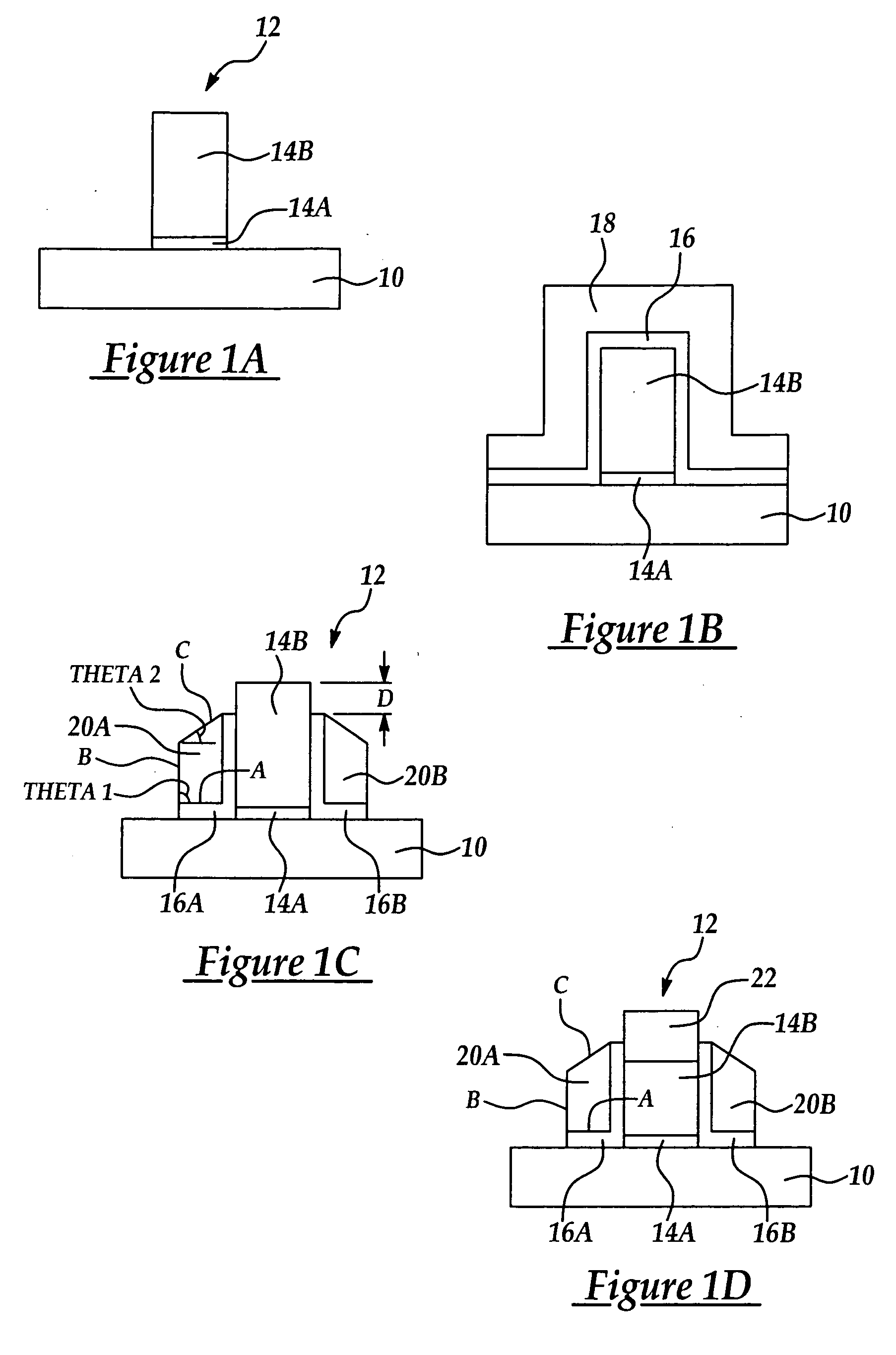
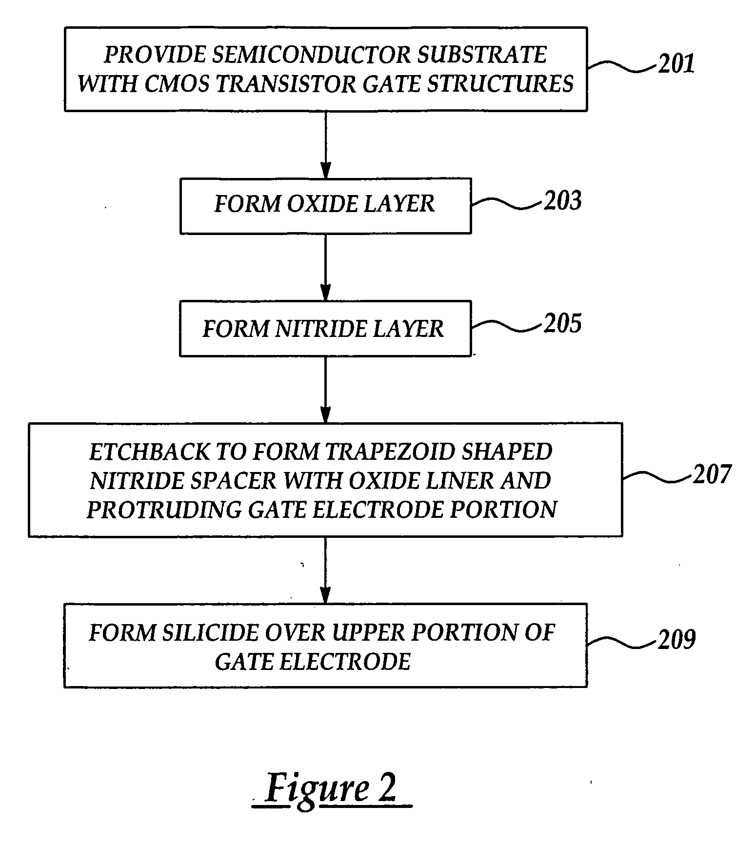
[0014] Although the method of the present invention is explained by reference to an exemplary CMOS transistor where the method of the present invention may be advantageously used, it will be appreciated that the method and spacers of the present invention may be used in any CMOS transistor or MOSFET structure where the width of the spacers is resistant to width reduction in subsequent etching processes including dry etching.

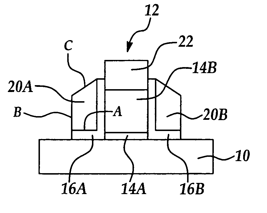
[0015] Referring to FIG. 1A is shown an exemplary implementation of the method of the present invention. Shown is a semiconductor substrate 10, having an overlying CMOS gate structure 12, including a gate dielectric portion 14A and overlying gate electrode portion 14B. Gate dielectric portion 14A and overlying gate electrode portion 14B are formed by conventional deposition, lithographic and etching processes. The substrate 10, for example, may include, but is not limited to, silicon, silicon on insulator (SOI), stacked SOI (SSOI), stacked SiGe on insulator (S-S...


PUM


Abstract

A CMOS device with trapezoid shaped spacers and a method for forming the same with improved critical dimension control and improved salicide formation, the CMOS device including a semiconductor substrate; a gate structure comprising a gate dielectric on the semiconductor substrate and a gate electrode on the gate dielectric; trapezoid shaped spacers adjacent either side of the gate structure; wherein, the trapezoid shaped spacers have a maximum height at an inner edge adjacent the gate electrode lower than an upper portion of the gate electrode to expose gate electrode sidewall portions.

Description

FIELD OF THE INVENTION [0001] This invention generally relates to processes for forming semiconductor devices including CMOS and MOSFET devices and more particularly to CMOS device spacers and a manufacturing method for forming the same to improve device performance including improved gate electrode electrical contact resistance (Rs). BACKGROUND OF THE INVENTION [0002] As MOSFET and CMOS device characteristic sizes are scaled below 0.1 microns including below 45 nm, the process window for wet and dry etching processes are increasingly difficult to control to achieve desired critical dimensions. For example, in forming dielectric spacers, also referred to as sidewall spacers or main spacers, it is particularly difficult to control the width of the spacers, especially when subjected to subsequent self aligned silicide (salicide) formation processes. For example, the width of a spacer may be as small as 600 Angstroms (60 nanometers) or less in 65 nanometer critical dimension (gate leng...

Claims


Application Information

Patent Timeline
IPC IPC(8): H01L21/8238
CPCH01L21/823864H01L29/665H01L29/6656H01L29/7833
Inventor TAO, HUN-JANHSU, JU-WANGLIANG, MONG-SONG
Owner TAIWAN SEMICON MFG CO LTD
Why Eureka
Try Eureka