Electrically floating body memory cell and array, and method of operating or controlling same

a memory cell and array technology, applied in semiconductor devices, digital storage, instruments, etc., can solve the problems of reducing device features, increasing the power consumption of memory cells, and relatively high bias voltages, and achieve the effect of facilitating memory cell programming

Inactive Publication Date: 2007-06-21
MICRON TECH INC
View PDF99 Cites 124 Cited by
  • Summary
  • Abstract
  • Description
  • Claims
  • Application Information

AI Technical Summary

Benefits of technology

[0020]In one aspect, the present inventions are directed to a semiconductor memory cell, memory cell array including a plurality of memory cells. In another aspect, the present inventions are directed to techniques for reading, controlling and/or operating, the memory cell and/or memory cell array. Each memory cell includes at least one transistor having an electrically floating body transistor and an active access element. The electrically floating body region of the transistor forms a storage area or node of the memory cell wherein an electrical charge which is representative of a data state i...

Problems solved by technology

Notably, conventional programming techniques may employ relatively high drain and/or gate bias voltages, which may increase the power cons...

Method used


Image

  • Electrically floating body memory cell and array, and method of operating or controlling same
  • Electrically floating body memory cell and array, and method of operating or controlling same
  • Electrically floating body memory cell and array, and method of operating or controlling same

Examples


Embodiment Construction

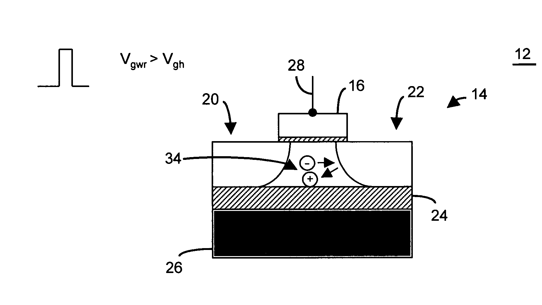
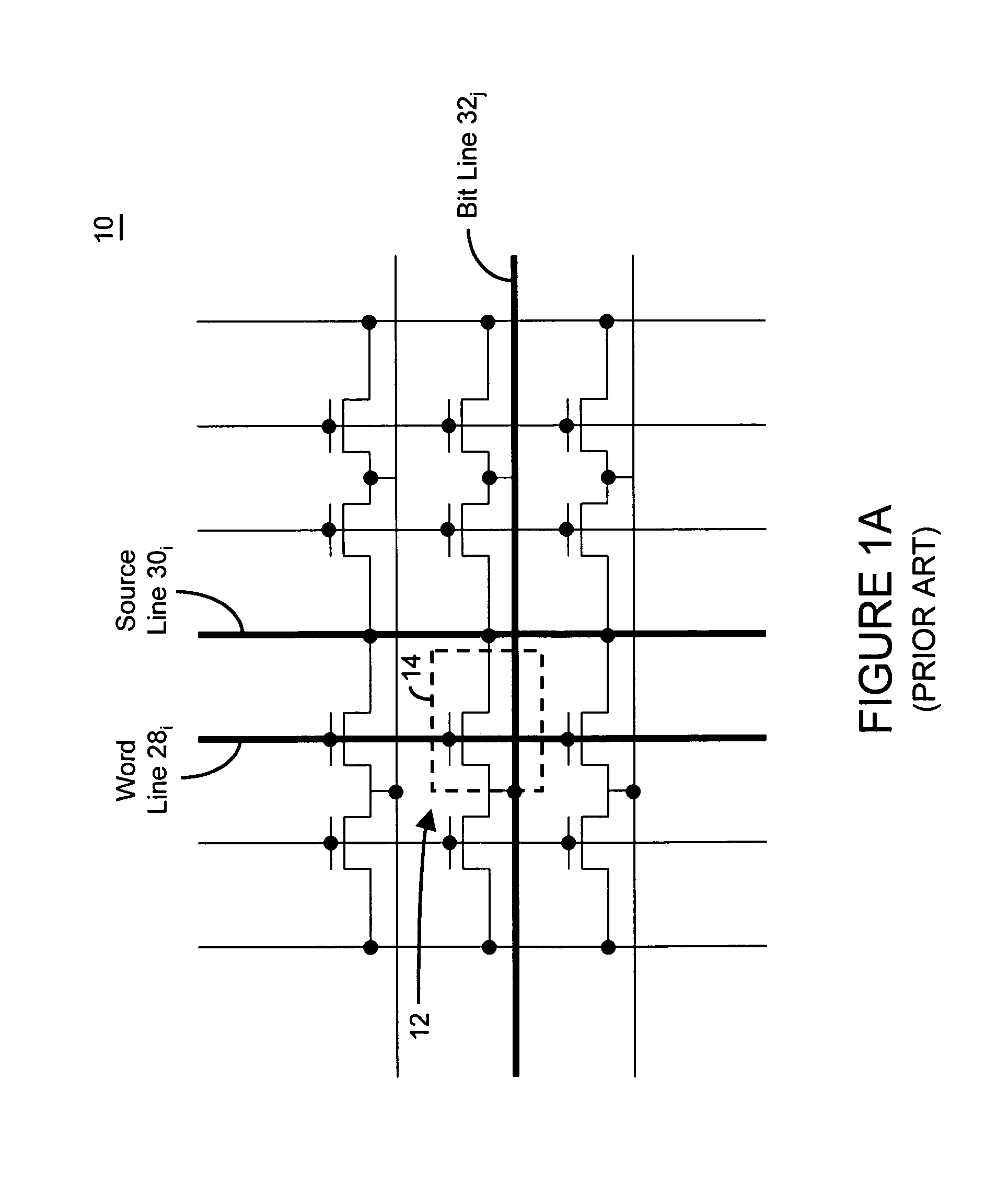
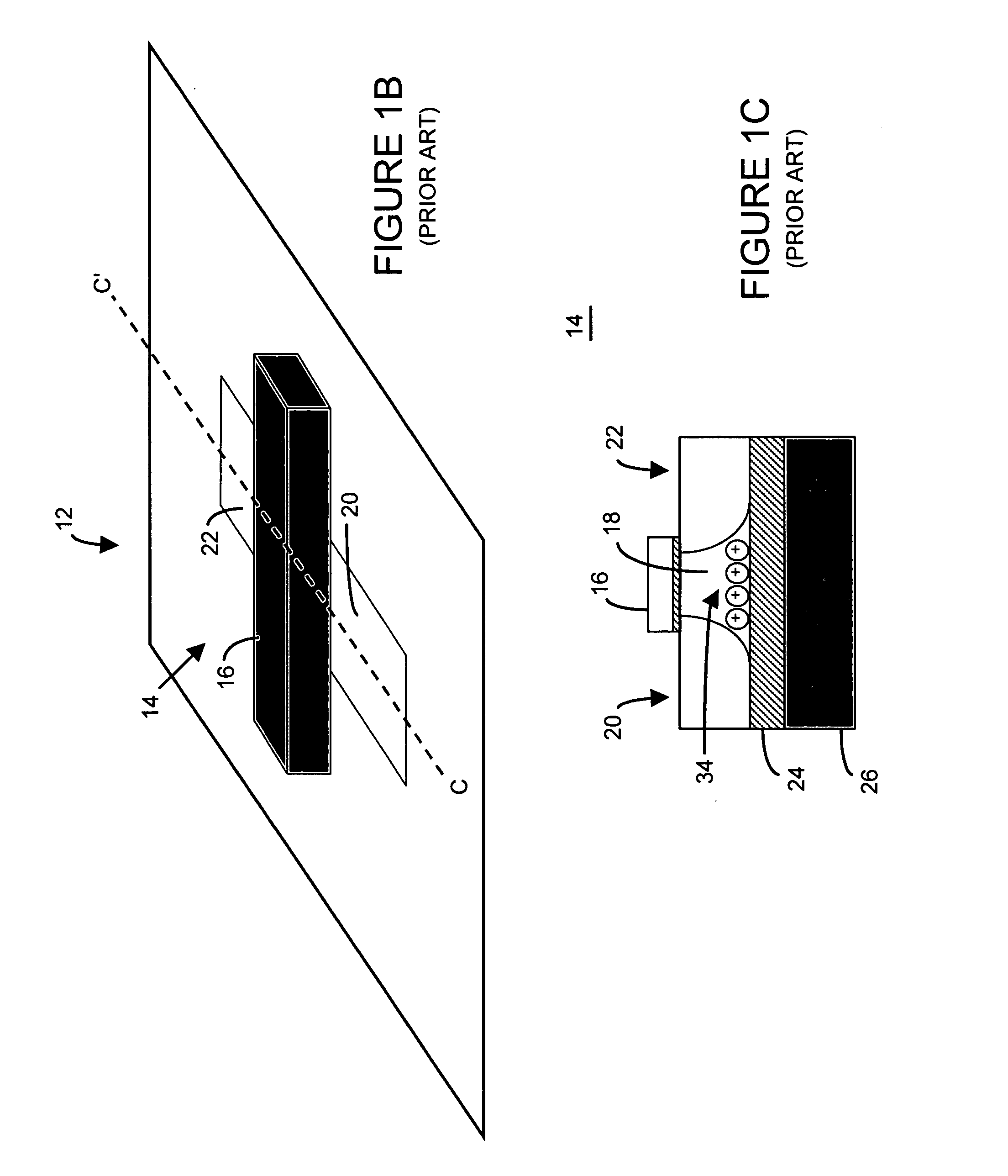
[0056]The present inventions describe a semiconductor memory cell, memory cell array, and techniques for reading, controlling and / or operating, the memory cell, and / or array. Each memory cell includes at least one transistor having an electrically floating body transistor and an active access element. The electrically floating body region of the transistor forms a storage area or node of the memory cell wherein an electrical charge which is representative of a data state is stored in the electrically floating body region. The active access element is coupled to the electrically floating body transistor to facilitate programming of the memory cell and to provide a relatively large amount of majority carriers to the storage area or node of the memory cell during a write operation. Notably, the memory cell and / or memory cell array of the present inventions may be incorporated in an integrated circuit device, for example, a logic device (such as, for example, a microcontroller or microp...


PUM


Abstract

An integrated circuit having a memory cell and/or memory cell array including a plurality of memory cells (as well as techniques for reading, controlling and/or operating, the memory cell, and/or memory cell array). Each memory cell includes at least one transistor having an electrically floating body transistor and an active access element. The electrically floating body region of the transistor forms a storage area or node of the memory cell wherein an electrical charge which is representative of a data state is stored in the electrically floating body region. The active access element is coupled to the electrically floating body transistor to facilitate programming of the memory cell and to provide a relatively large amount of majority carriers to the storage area or node of the memory cell during a write operation. The memory cell and/or memory cell array of the present inventions may be incorporated in an integrated circuit device, for example, a logic device (such as, for example, a microcontroller or microprocessor) or may comprise a portion of a memory device (such as, for example, a discrete memory).

Description

RELATED APPLICATION[0001]This application claims priority to U.S. Provisional Application Ser. No. 60 / 751,505, entitled “Floating Body Memory Cell and Array, and Method of Operating or Controlling Same”, filed Dec. 19, 2005; the contents of the provisional application are incorporated by reference herein in its entirety.BACKGROUND[0002]The inventions relate to a semiconductor memory cell, array, architecture and device, and techniques for reading, controlling and / or operating such cell and device; and more particularly, in one aspect, to a semiconductor dynamic random access memory (“DRAM”) cell, array, architecture and / or device wherein the memory cell includes an electrically floating body in which an electrical charge is stored.[0003]There is a continuing trend to employ and / or fabricate advanced integrated circuits using techniques, materials and devices that improve performance, reduce leakage current and enhance overall scaling. Semiconductor-on-Insulator (SOI) is a material i...

Claims


Application Information

Patent Timeline
IPC IPC(8): H01L29/94
CPCG11C5/025G11C11/404G11C2211/4016H01L27/108H01L27/10802H01L27/10826H01L27/1203H01L29/7841H01L29/785H10B12/20H10B12/36H10B12/00
Inventor OKHONIN, SERGUEI
Owner MICRON TECH INC
Why Eureka
Try Eureka