

Semiconductor device and method of manufacturing the same
a technology of semiconductors and semiconductors, applied in the direction of semiconductor devices, basic electric elements, electrical equipment, etc., can solve the problem of not being configured to reduce the on resistance sufficiently
- Summary
- Abstract
- Description
- Claims
- Application Information
AI Technical Summary
Problems solved by technology
Method used
Image

Examples
first embodiment
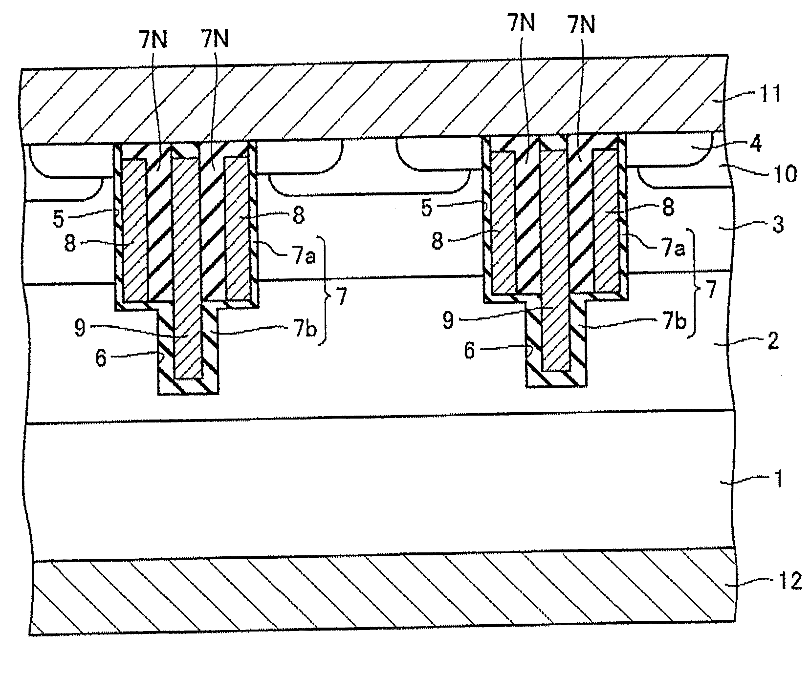
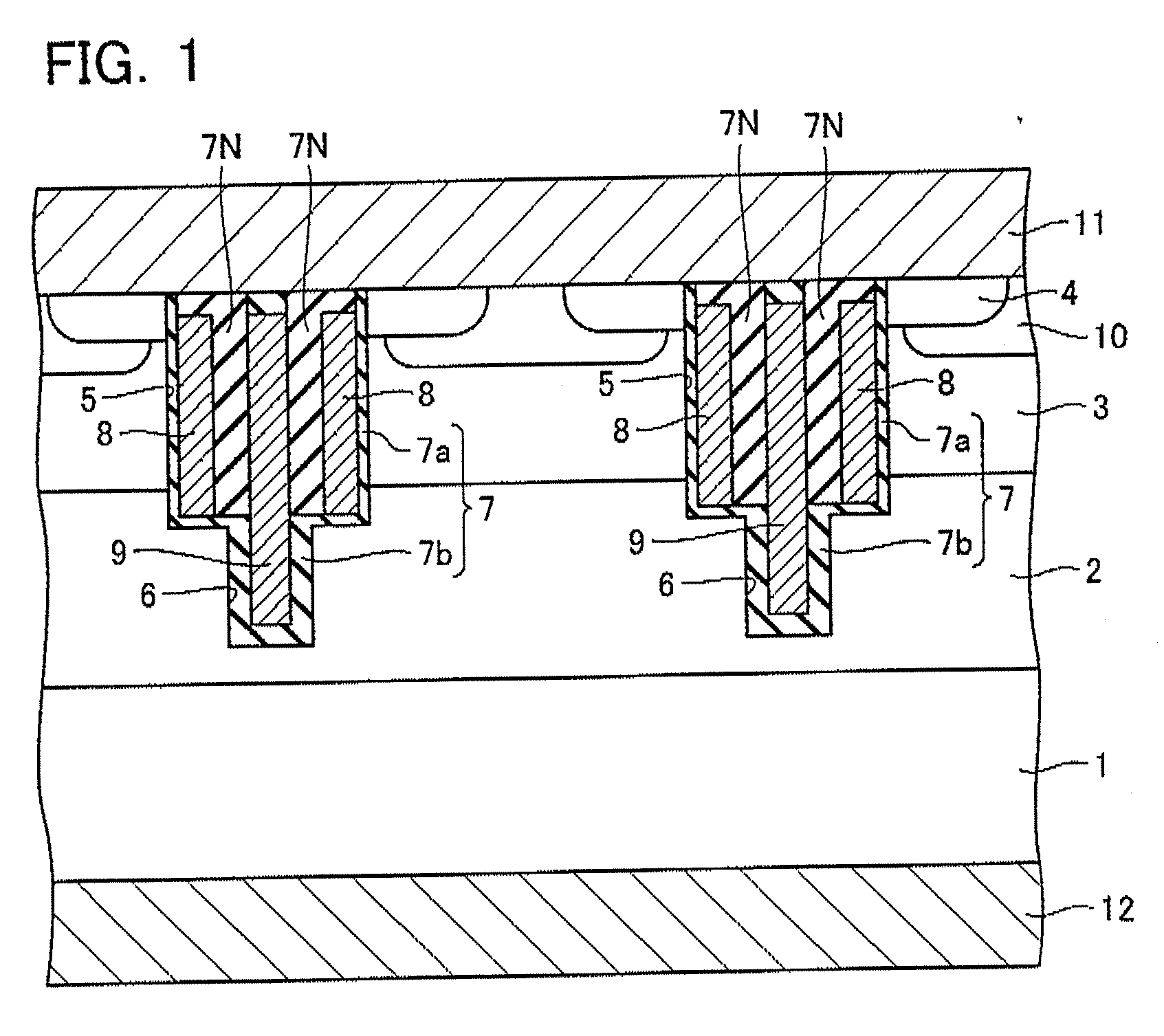
[0031]FIG. 1 is a cross-sectional view illustrative of a structure of a semiconductor device, or MOSFET, according to a first embodiment of the present invention. The semiconductor device according to the first embodiment mainly comprises an N+-type semiconductor substrate 1 an N−-type drift layer 2 formed over the N+-type semiconductor substrate 1, a P-type base layer 3 formed over the N−-type drift layer 2, and an N+-type source layer 4 formed in a surface of the P-type base layer 3.
[0032] A first trench 5 is formed from a surface of the N+-type source layer 4 through the P-type base layer 3 to a certain depth in the N−-type drift layer 2. A second trench 6 is formed near the center of the bottom of the first trench 5 much deeper than the first trench 5 to a certain depth in the N−-type drift layer 2.
[0033] An insulator film 7 is formed on sides of the first trench 5. A pair of gate electrodes 8, 8 are formed on the sides of the first trench 5 as spaced from each other with the ...
second embodiment
[0057] A semiconductor device according to a second embodiment of the present invention is described with reference to FIG. 13. As shown in FIG. 13A, the semiconductor device according to the second embodiment of the present invention is different from the first embodiment in a protruded electrode 9′. The protruded electrode 9′ is not formed at a depth opposite to the gate electrode 8 but is formed at a position much deeper than the depth where the gate electrode 8 is formed.
[0058] When Cgd is small and Cgs is large but does not result in self turn-on, the capacity between the protruded electrode 9′ and the gate electrode 8 increases the drive loss. Then, if the protruded electrode 9′ is not formed on the surface opposite to the gate electrode 7 as in the second embodiment, it is possible to reduce Cgs and improve the on resistance only. As shown in FIG. 13B, if an area at which the protrude electrode 9′ faces the gate electrode 8 is changed, it is possible to control Cgd / Cgs easil...
third embodiment
[0059] A semiconductor device according to a third embodiment of the present invention is described with reference to FIG. 14. As shown in FIG. 14, the semiconductor device according to the third embodiment of the present invention is different from the first embodiment in an N-type semiconductor layer 13 having a high impurity concentration and provided in a region where the protruded electrode 9 faces the N−-type drift layer 2.
[0060] The N-type semiconductor layer 13 is provided for the reason as described below. A terminal portion of the semiconductor device includes such a region that does not contain the first trench 5 and the second trench 6. When the impurity concentration is increased in the N−-type drift layer 2, a depletion layer can extend in the device portion to enhance the breakdown voltage, effected from the protruded electrode 9. In contrast, the breakdown voltage is lowered in the terminal portion because the protruded electrode 9 is not provided therein Therefore,...
PUM
 Abstract
Description
Claims
Application Information