Light emitting device

a technology of light-emitting devices and light-emitting components, which is applied in the direction of semiconductor devices, lighting and heating apparatus, instruments, etc., can solve the problems of insufficient heat dissipation, insufficient reliability in actual use, and large heat generation amounts, etc., to achieve wide viewing angles, high reliability, and high quality

Active Publication Date: 2007-06-21
NICHIA CORP
View PDF10 Cites 252 Cited by
  • Summary
  • Abstract
  • Description
  • Claims
  • Application Information

AI Technical Summary

Benefits of technology

[0010] According to a light emitting device of the present invention, it is possible to provi...

Problems solved by technology

However, there is a problem that the construction proposed in the above Publication has insufficient heat dissipation and cannot provide sufficient reliability in actual us...

Method used


Image

  • Light emitting device
  • Light emitting device
  • Light emitting device

Examples


Embodiment Construction

Light Emitting Device

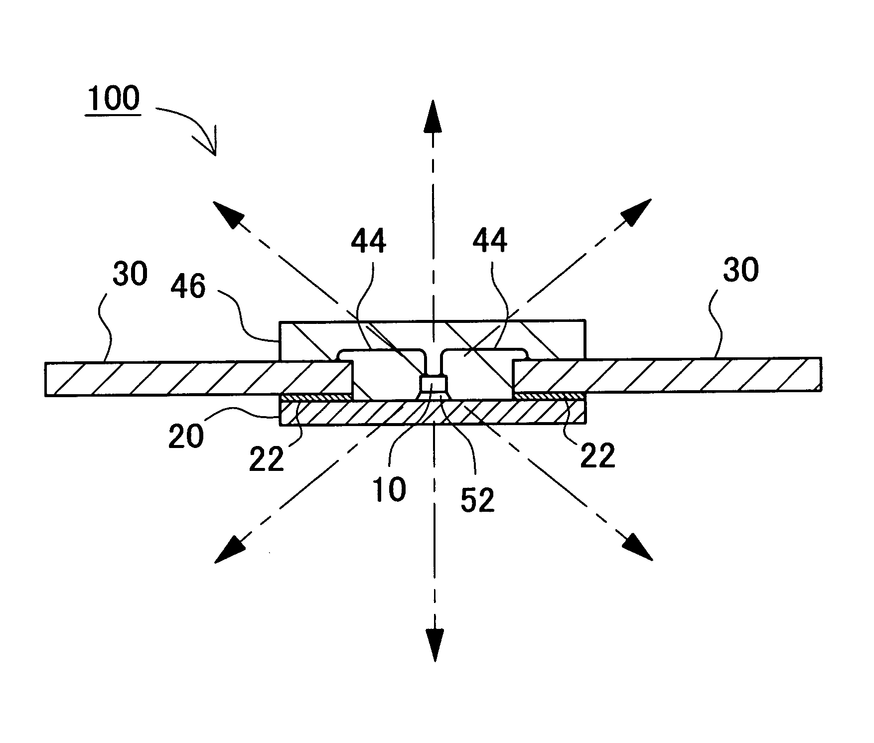
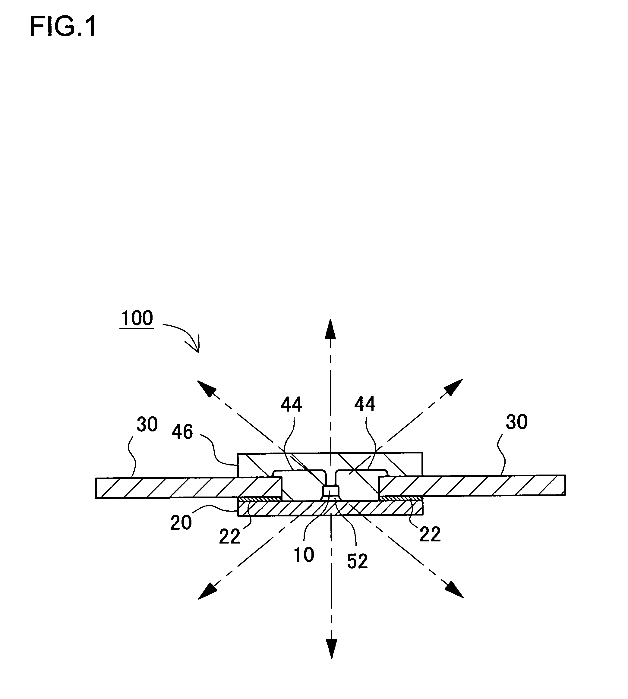
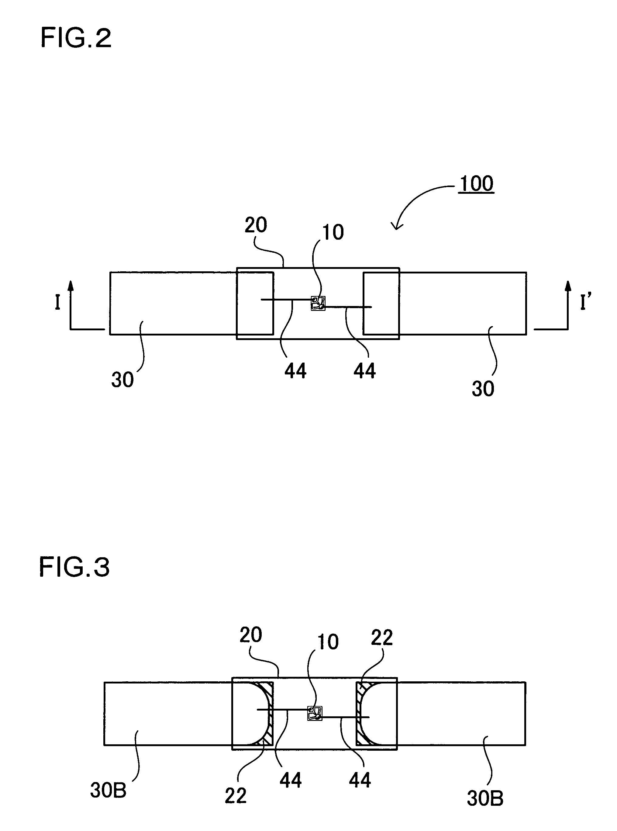
[0028]FIGS. 1 and 2 are views showing a light emitting device 100 according to a first embodiment of the present invention. FIG. 1 is a cross-sectional view showing the light emitting device 100. FIG. 2 is a plan view showing the light emitting device 100. FIG. 1 corresponds a cross-sectional view taken along the line I-I′ of FIG. 2. The light emitting device 100 illustrated in these Figures includes a light emitting element 10, a transparent board 20, a pair of conductor members 22, a covering member 46, and a pair of metal plates 30. The transparent board 20 is provided with the light emitting element 10 that is mounted thereon. The pair of conductor members 22 are secured on the transparent substrate 20. The covering member 46 is provided with the light emitting element 10 and the conductor members 22 that are located therein. The pair of metal plates 30 are inserted into the covering member 46 from side surfaces of the covering member 46, and are located o...


PUM


Abstract

Broad light emission is provided and additionally heat conductivity is increased to improve reliability. A light emitting device comprises a light emitting element, a pair of conductor members, a transparent board and a transparent member. The conductor members are spaced away from each other at an interval in a side-surface direction of the light emitting element and are electrically connected to the light emitting element. The transparent board supports the light emitting element and the pair of conductive members. The transparent member is located on the transparent board and seals the light emitting element and the pair of conductor members. The pair of conductor members are provided with a pair of metal plates that are secured thereon. The pair of metal plates project from the transparent member in directions different from each other.

Description

BACKGROUND OF THE INVENTION [0001] 1. Field of the Invention [0002] The present invention relates to a light emitting device that employs a semiconductor element such as light emitting diode and is mainly used in lighting applications, and a method for producing the light emitting device. [0003] 2. Description of the Related Art [0004] Light emitting devices that employ light emitting elements are small but high effective in terms of electric power consumption, and emit vivid color light. In addition, semiconductor elements are employed as the light emitting elements, thus, there are no concerns about bulb burnout and so on. Additionally, semiconductor elements have features, such as excellent initial drive characteristics, resistance to vibration or ON / OFF repeats. Since semiconductor elements have these excellent features, light emitting devices that employ semiconductor light emitting elements such as light emitting diode (hereinafter, occasionally referred to as “LED”) and semic...

Claims


Application Information

Patent Timeline
IPC IPC(8): G02B6/00H01L33/54H01L33/56H01L33/62H01L33/64
CPCF21K9/135F21Y2101/02H01L33/505H01L33/507H01L33/54H01L33/62H01L2224/48095H01L2224/73265H01L2924/01004H01L2924/0102H01L2924/01063H01L2924/01078H01L2924/01079H01L2224/32225H01L2224/48247H01L2924/00H05B33/04H01L2924/181F21K9/232F21Y2115/30F21Y2115/10F21Y2109/00F21V9/38F21V9/32F21V13/14H01L2924/00012F21Y2101/00F21V9/30F21V29/70F21K9/235F21V3/02F21V19/006F21V31/005H01L25/0753H01L33/501H01L33/508
Inventor TANDA, YUICHIROMATSUSHITA, TOSHIO
Owner NICHIA CORP
Why Eureka
Try Eureka