Nonvolatile semiconductor memory device

a semiconductor memory and non-volatile technology, applied in static storage, digital storage, instruments, etc., can solve problems such as readout errors, achieve the effects of avoiding any readout error of information, enabling acceleration of writing time, and reducing the effect of the threshold voltage difference between adjacent memory cells

Inactive Publication Date: 2007-06-21
SHARP KK
View PDF8 Cites 4 Cited by
  • Summary
  • Abstract
  • Description
  • Claims
  • Application Information

AI Technical Summary

Benefits of technology

[0037] According to the device of this invention, even when there exist memory cells from which information is excessively erased after erasure, the information is programmed to all the memory cells being a target of programming, and thus there is no need of programming back information to the memory cells from which information is excessively erased, thereby enabling acceleration of writing time.
[0038] In addition, since programming is performed so that the electrical attributes of all the memory cells being a target of programming may belong to any one of the distribution ranges for programming after erasing is performed so that the electrical attribute of the memory cell may belong to the distribution range for erasing, it is possible to eliminate extreme variation in the electrical attribute of the memory cell belonging to the distribution range corresponding to the specific data value, and consequently any readout error of the information can be avoided. Specifically, if the electrical attribute is threshold voltage, effect of variation in the threshold voltage between adjacent memory cells as described above can be avoided.
[0039] Furthermore, since it is judged whether or not the threshold voltage of the memory cell belongs to the distribution range for programming that corresponds to the desired data value, after the programming voltage is applied to all memory cells being a target of programming, any offset of the threshold voltage in unselected memory cells can be eliminated, consequently, the readout error of the information can be avoided.

Problems solved by technology

As these memory cells that are out of the second condition may cause various problems, there was need of finally eliminating them.
Hence, when writing of information has already completed in memory cells adjacent to the selected memory cells to be written, the threshold voltage of the adjacent memory cells also vary due to the variation in the threshold of the selected memory cells, thus possibly causing a readout error when information of the adjacent memory cells is read out.

Method used


Image

  • Nonvolatile semiconductor memory device
  • Nonvolatile semiconductor memory device
  • Nonvolatile semiconductor memory device

Examples


Embodiment Construction

[0049] In the following, based on the drawings, we describe embodiments of a nonvolatile semiconductor memory device (hereinafter abbreviated as the “device of this invention” as appropriate) according to the present invention.

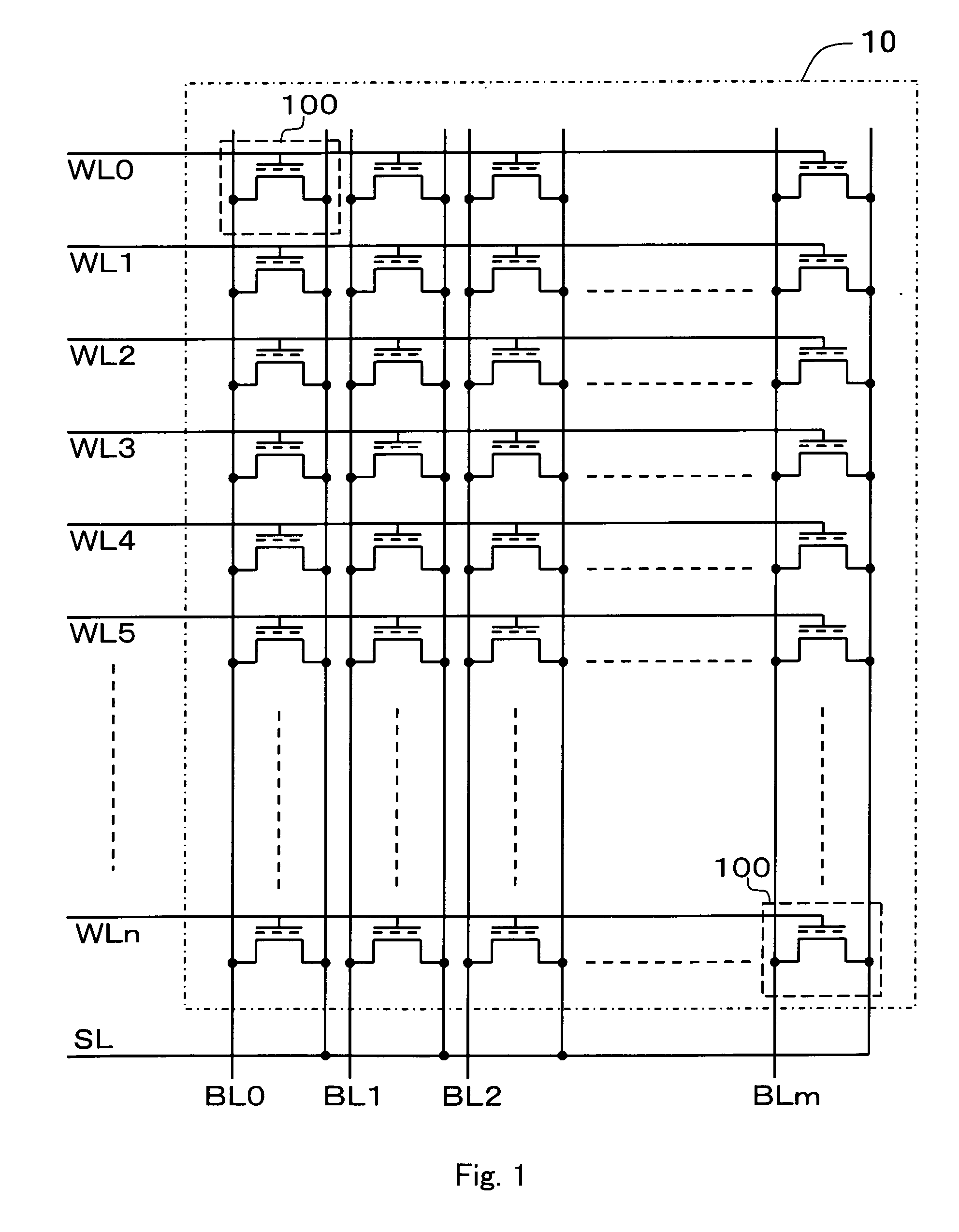
[0050]FIG. 4 is a block diagram showing schematic functional configuration of the device of this invention. FIG. 4 does not describe details of an input circuit for a plurality of address input signals, a plurality of data input signals, a plurality of control signals, etc., an output circuit for a plurality of data output signals, etc., a peripheral circuit such as a decoder circuit for address input signals, etc., as they are similar to those of a nonvolatile semiconductor memory device such as known flash memories, etc. Thus, FIG. 4 mainly describes circuit sections associated with a writing action of information by the memory cell array 10.

[0051] The device of this invention includes a memory cell array 10, a reference memory cell array 12, a word line v...


PUM


Abstract

There is provided a nonvolatile semiconductor memory device capable of accelerating writing time and avoiding readout errors of information by eliminating variation in threshold voltage of unselected memory cells. In a nonvolatile semiconductor memory device having a memory cell array with memory cells capable of erasing and programming information, the memory cells store one data value selected from the same number of data values as programming distribution ranges, associated with that the electrical attribute belongs to any one of the more than one programming distribution ranges. The device comprises an erasure means for erasing the selected memory cell to be erased so that its electrical attribute belongs to a erasure distribution range not overlapping any of the programming distribution ranges and a programming means for programming an erased memory cell to be programmed so that its electrical attribute belongs to any one of the programming distribution ranges.

Description

CROSS REFERENCE TO RELATED APPLICATION [0001] This Nonprovisional application claims priority under 35 U.S.C. §119(a) on Patent Application No. 2005-363000 filed in Japan on 16 Dec., 2005, the entire contents of which are hereby incorporated by reference. BACKGROUND OF THE INVENTION [0002] 1. Field of the Invention [0003] The present invention relates to a nonvolatile semiconductor memory device, and, more specifically, to a nonvolatile semiconductor memory device having a memory cell array arranged with a plurality of memory cells that can store information as a result of changed electrical attributes and erase and program the information by electrically changing the electrical attributes. [0004] 2. Description of the Related Art [0005] Recently, flash memories have become mainstream of nonvolatile semiconductor memory devices having a memory cell array arranged with a plurality of memory cells that can electrically erase and program information. The most general flash memories inc...

Claims


Application Information

Patent Timeline
Patent Type & Authority Applications(United States)
IPC IPC(8): G11C16/04G11C11/34
CPCG11C11/5628G11C11/5635G11C16/3404G11C16/3409G11C16/3413G11C16/344G11C16/3445G11C16/3454G11C16/3459G11C2211/5621
Inventor KANEKO, SEIJIUEDA, NAOKI
Owner SHARP KK
Why Eureka
Try Eureka