Semiconductor light emitting diode and method for manufacturing the same

Inactive Publication Date: 2007-06-28
SAMSUNG ELECTRONICS CO LTD
View PDF6 Cites 20 Cited by
  • Summary
  • Abstract
  • Description
  • Claims
  • Application Information

AI Technical Summary

Benefits of technology

[0011]An object of the present invention is to provide a high-efficiency semiconductor LED having a three-dimensional light-emitting stack structure, which can reduce the bad effect caused by the crystal defect.
[0012]Another object of th

Problems solved by technology

Therefore, in order to develop a semiconductor LED for illumination, the low efficiency of the semiconductor LED must be increased.
It has been known that this phenomenon is caused by carrier overflowing phenomenon and a reduced recombination efficiency due to the increase of a piezoelectric field at the quantum well.
However, if the size of the semiconductor LED chip is reduced, the price of the LED increases and its yield rapidly decreases.
Thus, the reduction in the size of the semiconductor LED chip is not an approach suitable for improving the internal quantum efficiency.
However, if the three-

Method used


Image

  • Semiconductor light emitting diode and method for manufacturing the same
  • Semiconductor light emitting diode and method for manufacturing the same
  • Semiconductor light emitting diode and method for manufacturing the same

Examples


second embodiment

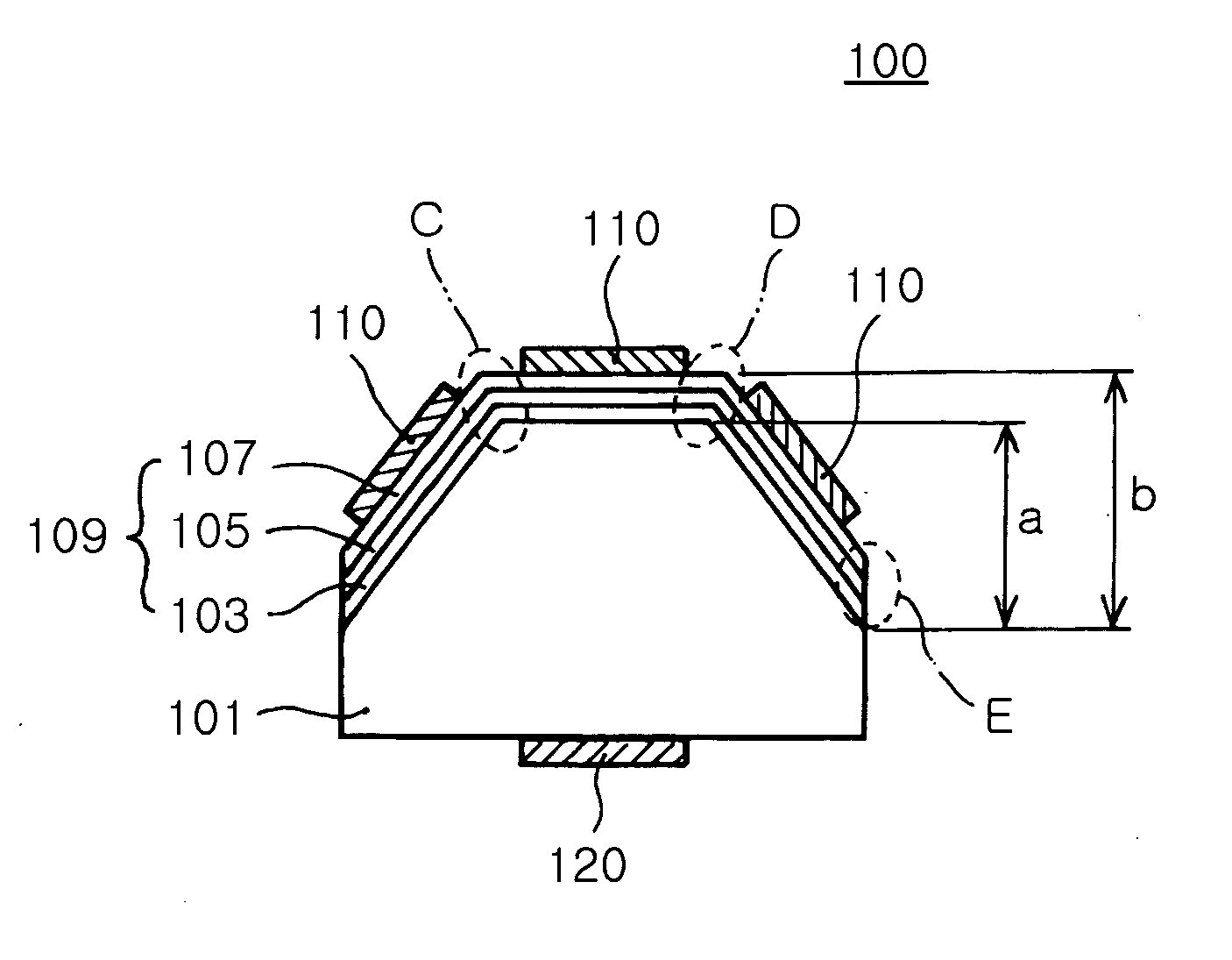
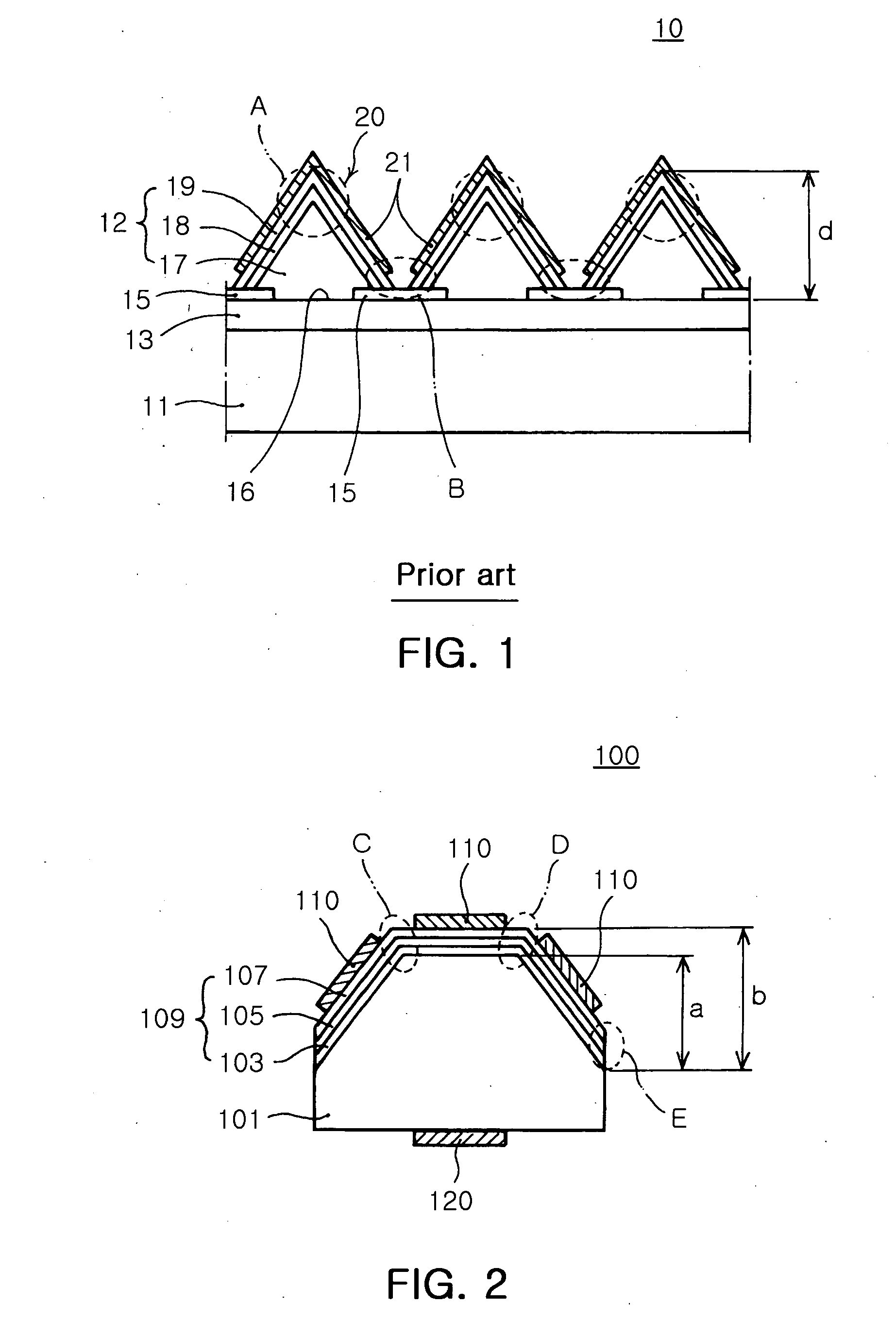
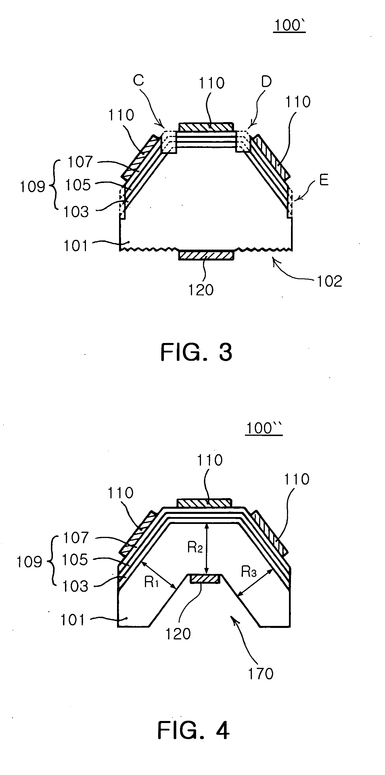
[0051]FIG. 3 is a sectional view of a semiconductor LED according to the present invention. In the semiconductor LED 100′ of FIG. 3, edges C, D and E of a three-dimensional light-emitting stack structure are removed using an etching process. By removing the edges C, D and E, a large amount of crystal defect existing in the edges is also removed. Thus, the bad effect caused by the crystal defect can be reduced or suppressed. A passivation layer (150 in FIG. 12) may be formed at the regions where the edges C, D and E are removed. The passivation layer may be formed of insulating material such as SiO2. The passivation layer can prevent the p-electrode 110 and the active layer 105 from being directly contacted with each other and can interrupt a undesired current flowing through the edges C, D and E.

[0052]The GaN-based substrate 101 may have an uneven bottom surface 102, which is a light exit surface. The uneven bottom surface 102 provides a roughness. The uneven bottom surface 102 redu...

third embodiment

[0053]FIG. 4 is a sectional view of a semiconductor LED according to the present invention. In the semiconductor LED 100″ of FIG. 4, a groove 170 is formed in a bottom surface of a substrate 101. The groove 170 reduces a deviation of thickness R1, R2 and R3 of the substrate 101. Because a deviation of current paths passing through the substrate 101 is reduced, the current can flow more uniformly. Consequently, the operating voltage is lowered and a local concentration of the current density can be prevented. That is, the groove 170 formed in the bottom surface of the substrate 101 functions to accelerate a current diffusion. The semiconductor LED 100″ also has the above-described advantages.

[0054]FIG. 5 is a sectional view of a semiconductor LED according to a fourth embodiment of the present invention. Referring to FIG. 5, a groove 170 is formed in a bottom surface of a substrate 101 so as to reduce a thickness deviation of the substrate 101. Also, the substrate 101 has an uneven b...

first embodiment

[0061]FIGS. 7 to 12 are sectional views illustrating a method for manufacturing a semiconductor LED according to the present invention.

[0062]Referring to FIG. 7, a GaN-based substrate 101 is prepared. Instead of the GaN-based substrate, other conductive substrates such as a SiC substrate may be used. It is preferable that the conductive substrate has a thickness of more than 50 μm. Referring to FIG. 8, the GaN-based substrate 101 is processed such that its top surface has a plurality of three-dimensional shapes. For example, a plurality of trapezoidal pyramid structures may be formed on the top surface of the substrate 101 by sawing the substrate 101 using a wheel, or scribing the substrate 101 using a diamond pencil.

[0063]It is preferable that the substrate is processed to have the three-dimensional shape of 10-100 μm in size. Also, it is preferable that the top surface of the processed substrate has at least one of c-plane, a-plane, n-plane. The reason for this is that the nitride...


PUM


Abstract

A high-efficiency semiconductor light emitting diode and a method for manufacturing the same are provided. The semiconductor LED has high internal quantum efficiency and can reduce the bad effect caused by the crystal defect. In the semiconductor light emitting diode, a conductive substrate has a three-dimensional top surface, and a light-emitting stack structure has a three-dimensional structure and includes an n-type nitride semiconductor layer, an active layer, and a p-type nitride semiconductor layer, which are sequentially formed on the conductive substrate. A p-electrode is formed on the p-type nitride semiconductor layer, and an n-electrode is formed on a bottom surface of the conductive substrate.

Description

RELATED APPLICATION[0001]The present application is based on, and claims priority from, Korean Application Number 2005-132250, filed Dec. 28, 2005, the disclosure of which is hereby incorporated by reference herein in its entirety.BACKGROUND OF THE INVENTION[0002]1. Field of the Invention[0003]The present invention relates to a semiconductor light emitting diode (LED), and more particularly, to a high-efficiency nitride semiconductor LED with a three-dimensional light-emitting stack structure.[0004]2. Description of the Related Art[0005]Recently, display devices and illuminating devices using semiconductor LEDs such as GaN-based LEDs have been actively developed for low power, high efficiency, high color reproduction, fast response speed, and environmental affinity. Since the semiconductor LED does not reach 801 m / W, which is the efficiency of a fluorescent lamp, it does not still replace the fluorescent lamp used for general illumination. The semiconductor LED is used in a light so...

Claims


Application Information

Patent Timeline
IPC IPC(8): H01L33/00H01L33/20H01L33/22H01L33/24
CPCH01L33/20H01L33/22H01L33/24
Inventor CHOI, PUN JAESONG, SANG YEOBHONG, SUK YOUN
Owner SAMSUNG ELECTRONICS CO LTD
Why Eureka
Try Eureka