Electrophoretic display device and electronic apparatus

a display device and display layer technology, applied in static indicating devices, non-linear optics, instruments, etc., can solve the problems of reliability defect, increase the electrical conductivity of the display layer, degrade the display function, etc., and achieve high reliability and high quality

Active Publication Date: 2007-06-28
E INK CORPORATION
View PDF2 Cites 14 Cited by
  • Summary
  • Abstract
  • Description
  • Claims
  • Application Information

AI Technical Summary

Benefits of technology

[0034] Since the electronic apparatus includes the electrophoretic display device c...

Problems solved by technology

On the other hand, a microcapsule-type electrophoretic device is disadvantageous in that when moisture or the like enters a microcapsule display layer from the outside, the electric conductivity of the display layer is increased to degrade the display function.
Thi...

Method used


Image

  • Electrophoretic display device and electronic apparatus
  • Electrophoretic display device and electronic apparatus
  • Electrophoretic display device and electronic apparatus

Examples


first embodiment

[0047] The present invention will be described in detail below.

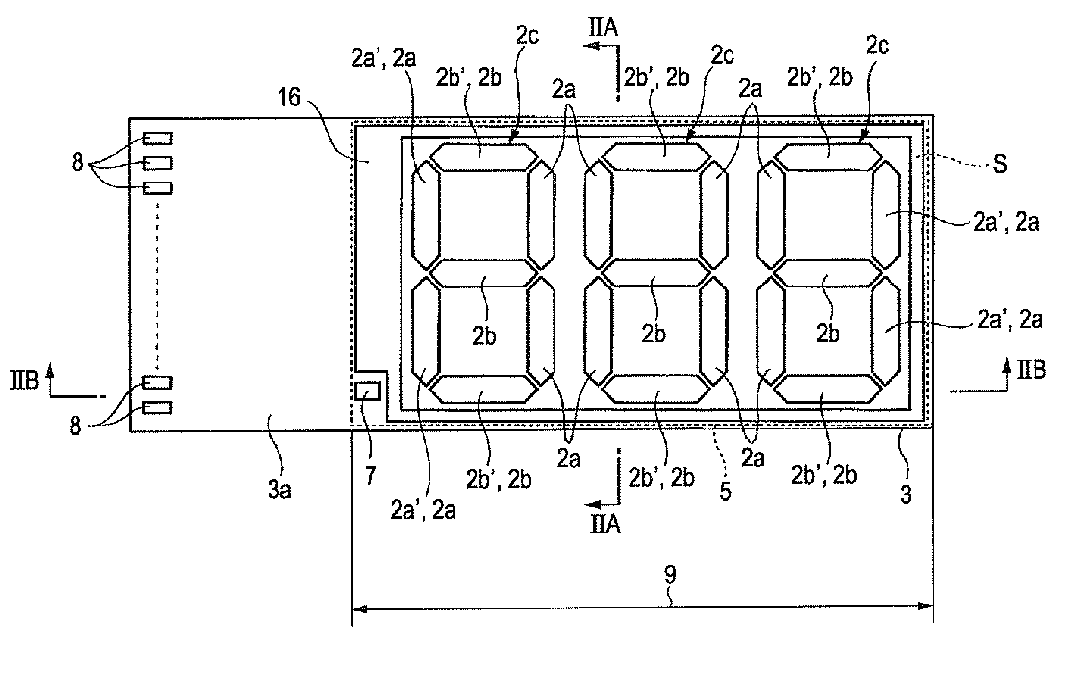
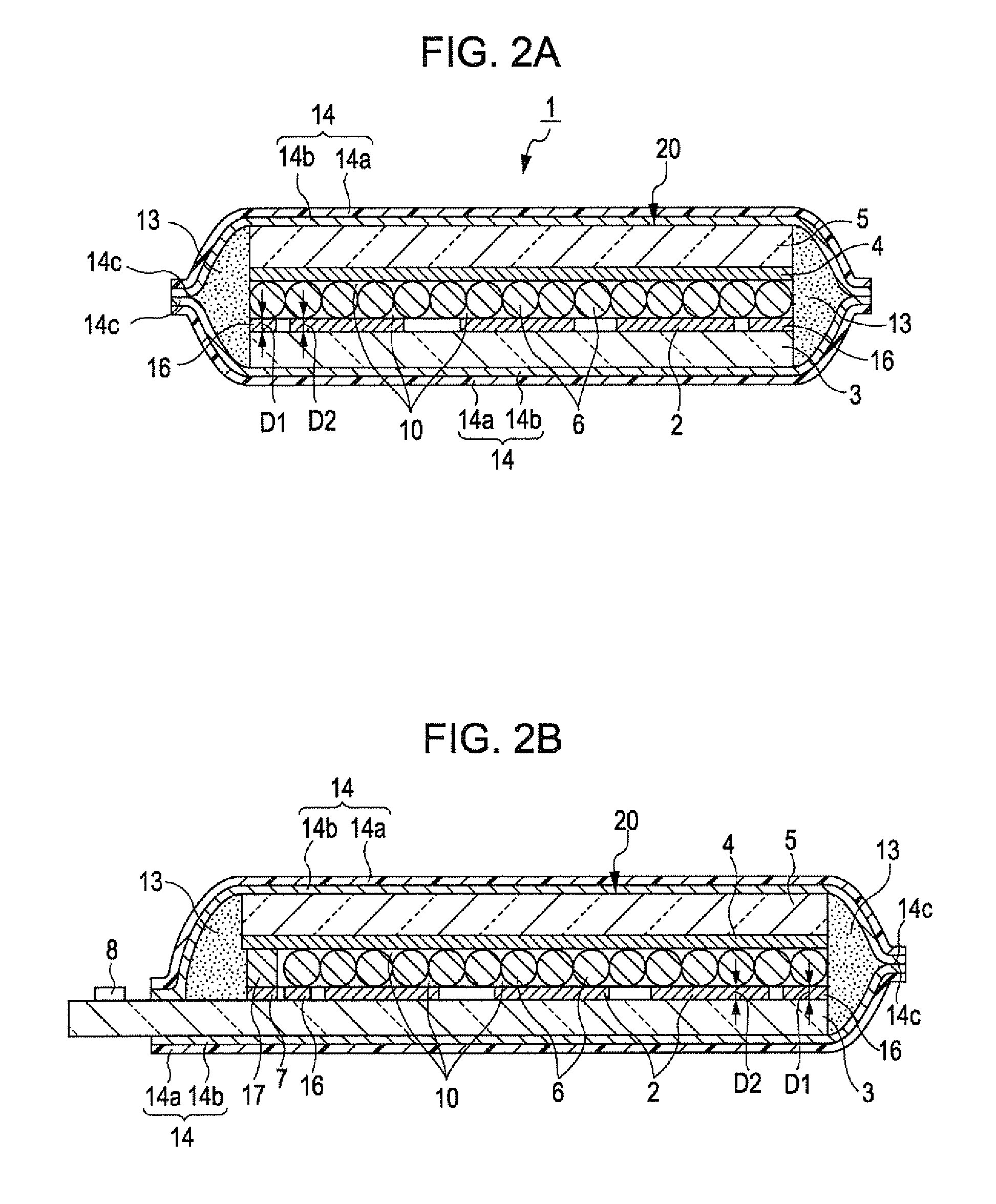
[0048]FIG. 1 shows an electrophoretic display device according to an embodiment of the invention. In FIG. 1, reference numeral 1 denotes an electrophoretic display device. FIG. 2A is a sectional view of the electrophoretic display device 1 taken along line IIA-IIA in FIG. 1. FIG. 2B is a sectional view of the electrophoretic display device 1 taken along line IIB-IIB in FIG. 1. In each of the drawings used for description below, the scales of layers and members are different for showing the layers and members in respective recognizable sizes. In this embodiment, the opposing surfaces of first and second substrates 3 and 5 are referred to as “the inner surfaces”, and the surfaces opposite to the inner surfaces are referred to as “the outer surfaces”.

(Electrophoretic Display Device)

[0049] As shown in FIGS. 2A and 2B, the electrophoretic display device 1 includes a display element 20 and waterproof sheets 14 (protective ...

second embodiment

[0098] A second embodiment will be described with reference to the drawings.

[0099] In the first embodiment, the dummy electrode 16 composed of the same material as that of the pixel electrodes is formed as the spacer for filling the step. However, the second embodiment is different from the first embodiment in that a solder resist is used as a spacer for protecting lead wiring or the like. The other basic components of an electrophoretic display device are the same as in the first embodiment. The common components are denoted by the same reference numerals, and the detailed description thereof is omitted.

[0100]FIG. 4 is a sectional view showing the schematic configuration of an electrophoretic display device in which a dummy pattern 22 is formed. As shown in FIG. 4, the terminals 8 are formed in the projecting portion 3a of the first substrate 3, for mounting FPC. In addition, a solder resist (not shown) is disposed in the periphery of the terminals 8, for preventing the adhesion ...

third embodiment

[0105] Next, a third embodiment will be described with reference to the drawings.

[0106] The third embodiment is different from the first embodiment in that a copper pattern 24 and a resist film 26 are formed on the outer surface of at least one of first and second substrates 3 and 5. The other basic components of an electrophoretic display device are the same as in the first embodiment. The common components are denoted by the same reference numerals, and the detailed description thereof is omitted.

[0107]FIGS. 5A and 5B are sectional views showing the schematic configuration of an electrophoretic display device 1 in which a reinforcing member 28 is formed.

[0108] The reinforcing member 28 is formed on the outer surface of the first substrate 3, for improving rigidity of the first substrate 3. As shown in FIGS. 5A and 5B, the reinforcing member 28 is formed so as to partially planarly overlap the dummy electrode 16 (dummy pattern 22) formed on the inner surface of the first substra...


PUM


Abstract

An electrophoretic display device includes a display element including a pair of first and second substrates which are opposed to each other, and a microcapsule enclosing a display material changed in optical characteristics in response to an electric impulse, the microcapsule being sandwiched between the first and second substrates; and a protective film sealing the display element. In the display device, a first electrode is provided on the surface of the first substrate which faces the second substrate, a second electrode is provided on the surface of the second substrate which faces the first substrate, and a spacer is provided in the space between the periphery of the facing surface of the first substrate and the first electrode.

Description

BACKGROUND [0001] 1. Technical Field [0002] The present invention relates to an electrophoretic display device and an electronic apparatus. [0003] 2. Related Art [0004] There have been known electrophoretic display devices each including an electrophoretic dispersion liquid containing a liquid phase dispersion medium and electrophoretic particles and using the phenomenon that when an electric field is applied, the dispersion state of the electrophoretic particles is changed to change the optical characteristics of the electrophoretic dispersion liquid (refer to, for example, Japanese Unexamined Patent Application Publication No. 6203954). Such electrophoretic display devices may be decreased in cost and thickness due to no need for backlight. Furthermore, the electrophoretic display devices have a wide angle of view, high contrast, and display memory, and thus the electrophoretic display device attract attention as next-generation display devices. [0005] A known example of such elec...

Claims


Application Information

Patent Timeline
IPC IPC(8): G09G3/34G02F1/167G02F1/16757
CPCG02F1/167G09G3/344G02F2201/50G02F1/1339G02F1/16757
Inventor UCHIDA, MASAMI
Owner E INK CORPORATION
Why Eureka
Try Eureka