Optical touch pad with multilayer waveguide

a multi-layer waveguide and optical touch technology, applied in the field of optical touch pads, can solve the problems of increasing the overall size of the device to which it is attached, increasing the overall size of the device, and not providing adequate ruggedness to endure the standard use conditions of some devices, so as to reduce optical noise

Inactive Publication Date: 2007-07-05
FLATFROG LAB
View PDF44 Cites 187 Cited by
  • Summary
  • Abstract
  • Description
  • Claims
  • Application Information

AI Technical Summary

Benefits of technology

[0010] The plurality of waveguide layers may include two or more layers having progressively lower refractive indices towards a border between two refractive indices that form a total internal reflection mirror that confines the optical touch pad from optical interference caused by the display and / or other surfaces beneath the optical touch pad. In some instances, at least one or more of the indices of refraction may be selected to significantly reduce optical noise within the multilayer waveguide caused by surface contaminants.

Problems solved by technology

However, conventional touch pad systems may be bulky, and may increase an overall size of a device to which it may be attached.
Additionally, conventional touch pads may not provide adequate ruggedness to endure standard use conditions in some devices, such as personal mobile devices like radio telephones, PDA's, and / or other personal mobile devices.
In general, the addition of a typical touch pad to a conventional flat panel display, and / or other conventional displays, may also result in degradation of display performance.
For example, these and other drawbacks may be associated with optical touch pads that implement light emitting styluses, optical touch pads that implement frustrated internal resistance supplied to the optical touch pad by a dedicated light source, optical touch pads that implement coordination with the rasterization of a CRT display to determine positional information related to an object, and optical touch pads that utilize an imaging device that images the surface of the optical touch pad.

Method used


Image

  • Optical touch pad with multilayer waveguide
  • Optical touch pad with multilayer waveguide
  • Optical touch pad with multilayer waveguide

Examples


Embodiment Construction

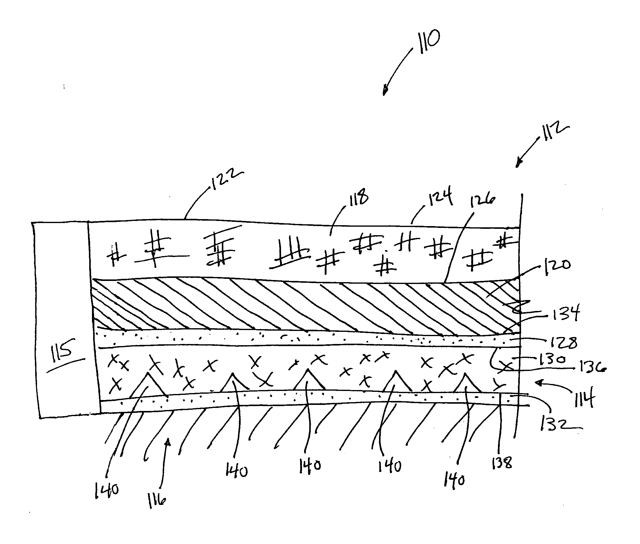
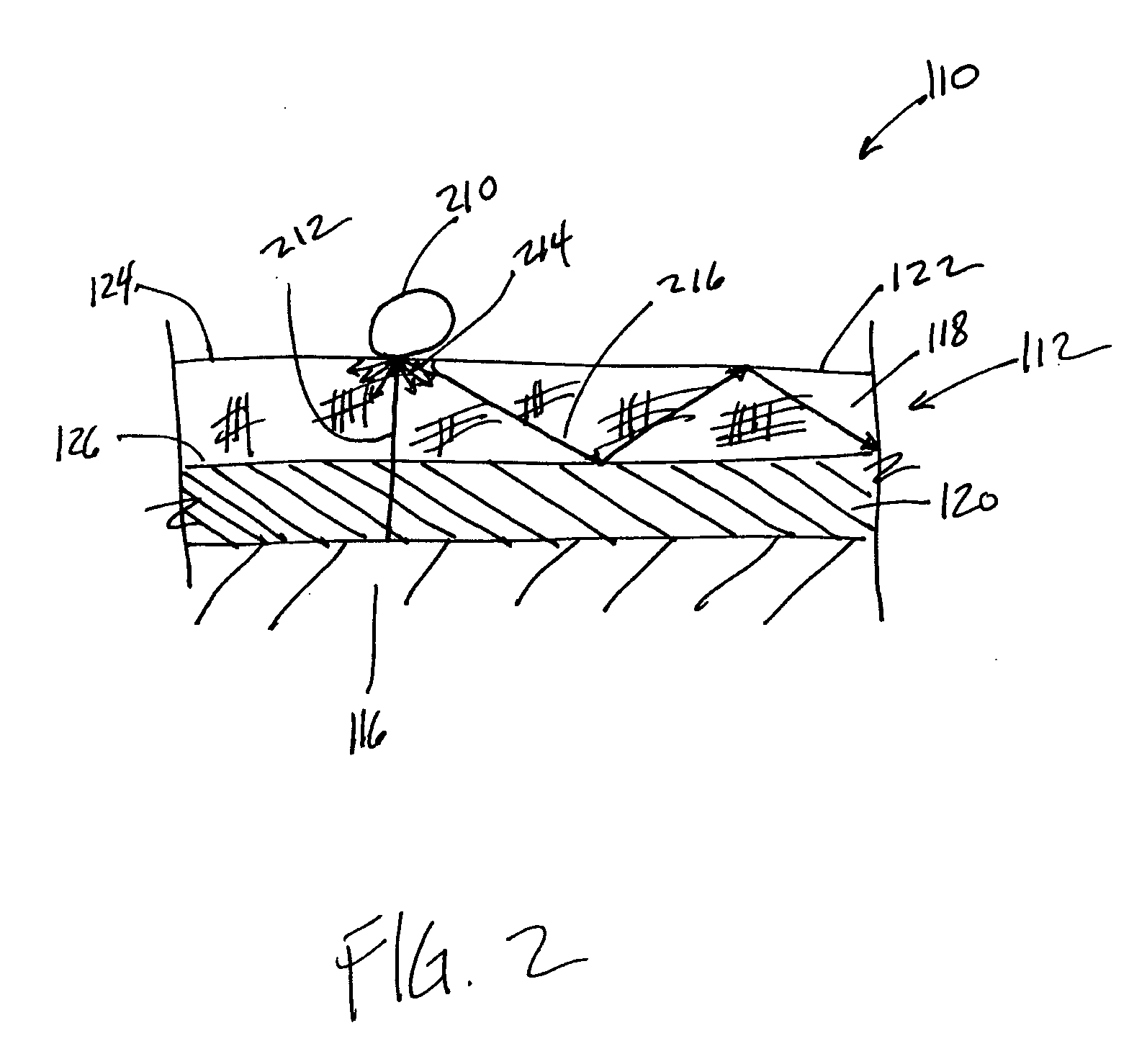
[0029]FIG. 1 illustrates a cross section of an optical touch pad 110 in accordance with one or more implementations of the invention. As is shown in FIG. 1, touch pad 110 may include a multilayer waveguide 112, at least one detector 115, and one or more additional layers. In some implementations, multilayer waveguide 112 may be optically coupled to at least one detector 115. Optical touch pad 110 may be mounted on a display 116. Display 116 may include an electronic display (e.g., a CRT display, an LCD display, a micro-mirror display, etc.), or other types of displays. In some implementations, display 116 may include a base object that does not emit electromagnetic radiation. For example display 116 may include a printed image over which optical touch pad 110 may be disposed, or display 116 may provide a surface for mounting optical touch pad 110 to that includes no image or electronic display. Other forms of display 116 may exist.

[0030] In some implementations, multilayer waveguid...


PUM


Abstract

An optical touch pad that includes a multilayer waveguide optically coupled to at least one electromagnetic radiation detector. Based on electromagnetic radiation directed from an object to the detector by the multilayer waveguide, information related to an object proximate to (e.g., hovering above) and / or in contact with the optical touch pad may be determined. For example, the information related to the object may include position information, object-type information, and / or other information related to the object.

Description

FIELD OF THE INVENTION [0001] The invention relates to optical touch pads that use total internal reflection to direct electromagnetic radiation returned to an optical touch pad from an object to determine positional information, and / or other information related to the object. BACKGROUND OF THE INVENTION [0002] Touch pad systems that enable a user to input information to a processor by moving an object relative to a touch pad surface are known. Typically, touch pads may be implemented in computing applications such as PDA's and computers, and may also be found in electronic displays in a wide variety of applications such as teller machines, gaming machines, automotive navigation systems, restaurant management systems, grocery store checkout lines, gas pumps, information kiosks, and hand-held data organizers, to name a few. [0003] However, conventional touch pad systems may be bulky, and may increase an overall size of a device to which it may be attached. Additionally, conventional ...

Claims


Application Information

Patent Timeline
Patent Type & Authority Applications(United States)
IPC IPC(8): G06F3/042
CPCG06F2203/04109G06F3/0421
Inventor OSTERGAARD, JENS WAGENBLAST STUBBEELIASSON, JONAS OVE PHILIPBASTUE, JENS
Owner FLATFROG LAB
Why Eureka
Try Eureka