Eureka AIR delivers breakthrough ideas for toughest innovation challenges, trusted by R&D personnel around the world.

Display substrate and method of manufacturing the same

Active Publication Date: 2007-07-05
SAMSUNG DISPLAY CO LTD
View PDF8 Cites 5 Cited by
  • Summary
  • Abstract
  • Description
  • Claims
  • Application Information

AI Technical Summary

Benefits of technology

[0010] According to the display substrate and the method of manufacturing the same mentioned above, the metallic conductors have a double-layer structure (Mo / Al) including a lower layer of molybdenum (Mo) or a molybdenum alloy and an upper layer of aluminum (Al) or an aluminum alloy, to prevent deterioration of the conductors.

Problems solved by technology

Moreover, when the screen size and resolution of the LCD device are increased, the resistive-capacitive (RC) delay of the metallic conductors formed on the display substrate is increased.
The aluminum conductors reduce the RC delay, however, the number of defects generated during manufacturing of the LCD device typically increase.

Method used


Image

  • Display substrate and method of manufacturing the same
  • Display substrate and method of manufacturing the same
  • Display substrate and method of manufacturing the same

Examples


Embodiment Construction

[0019] It will be understood that when an element or layer is referred to as being “on,”“connected to” or “coupled to” another element or layer, it can be directly on, connected or coupled to the other element or layer or intervening elements or layers may be present. In contrast, when an element is referred to as being “directly on,”“directly connected to” or “directly coupled to” another element or layer, there are no intervening elements or layers present. Like numbers refer to like elements throughout. As used herein, the term “and / or” includes any and all combinations of one or more of the associated listed items.

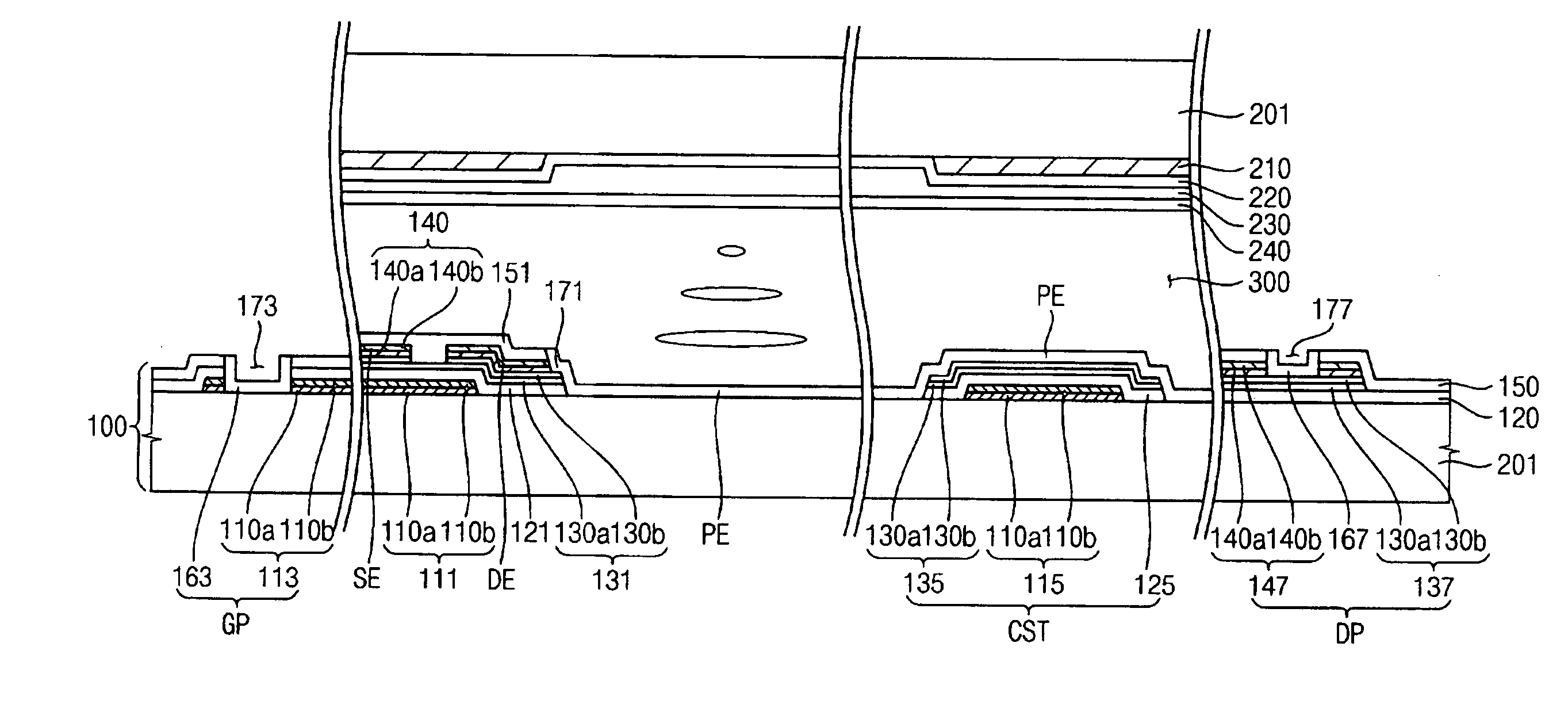
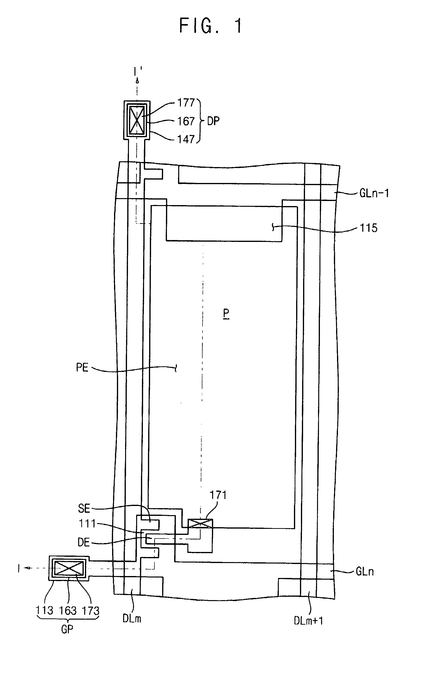
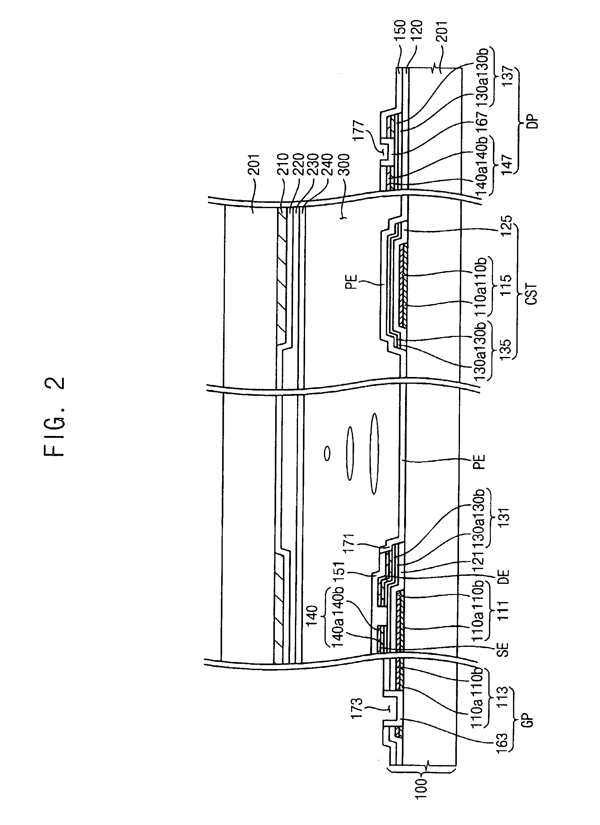
[0020]FIG. 1 is a schematic plan view illustrating a display panel in accordance with an embodiment of the present invention. FIG. 2 is a cross-sectional view illustrating the display panel taken along the line I-I′ in FIG. 1.

[0021] Referring to FIGS. 1 and 2, the display panel includes an array substrate 100, a color filter substrate 200 facing the array substrate 1...


PUM


Abstract

A display substrate having a low-resistance metallic layer and a method of manufacturing the display substrate. The gate conductors are extended in a first direction. The source conductors are extended in a second direction crossing the first direction including a lower layer of molybdenum or a molybdenum alloy, and an upper layer of aluminum or an aluminum alloy. The pixel areas are defined by the gate conductors and the source conductors. A switching element is formed in each of the pixel areas and includes a gate electrode extended from the gate conductor and a source electrode extended from the source conductor. The pixel electrode includes a transparent conductive material, and is electrically connected to a drain electrode of the switching element.

Description

CROSS-REFERENCE TO RELATED APPLICATIONS [0001] This application claims priority of Korean Patent Application No. 2006-205 filed on Jan. 2, 2006, the contents of which are herein incorporated by reference. [0002] 1. Field of the Invention [0003] The present invention relates to a display substrate and, more particularly, to a display substrate having low-resistance metallic conductors and a method of manufacturing the same. [0004] 2. Description of the Related Art [0005] In general, a liquid crystal display (LCD) includes a liquid crystal layer injected into the space between a display substrate and a counter substrate. [0006] Gate conductors, source conductors crossing the gate conductors, a switching element electrically connected to each of the gate conductors and each of the source conductors, and a pixel electrode electrically connected to the switching element are formed on the display substrate. The switching element includes a gate electrode extended from each of the gate con...

Claims


Application Information

Patent Timeline
IPC IPC(8): G02F1/136
CPCG02F1/136286H01L27/124G02F2001/136295G02F2001/13629G02F1/13629G02F1/136295E05C17/56E05Y2201/418E05Y2201/46E05Y2600/626E05Y2900/132
Inventor KIM, JOO-HANOH, MIN-SEOKLEE, JUN-YOUNGKANG, SUNG-WOOK
Owner SAMSUNG DISPLAY CO LTD
Why Eureka
Eureka Blog
Learn More