
Method and system for high power switching

Inactive Publication Date: 2007-07-12
RAYTHEON CO
View PDF6 Cites 5 Cited by
  • Summary
  • Abstract
  • Description
  • Claims
  • Application Information

AI Technical Summary

Benefits of technology

[0005] Embodiments of the invention may provide numerous technical advantages. Some, none, or all embodiments may benefit from the below-described advantages. According to one embodiment of the invention, a DC restoring circuit allows for switching of alternating current signals at high power levels through a small device with large absorption of RF energy and good insertion loss.

Problems solved by technology

In terms of power handling a switch field effect transistor (FET) is limited in its high impedance “off”state by the gate bias voltage used to control the device.
A problem with this approach is that a large number of stacked switch FETs in series creates a large circuit size and therefore is costly.
It also increases the insertion loss of the switch.

Method used


Image

  • Method and system for high power switching
  • Method and system for high power switching
  • Method and system for high power switching

Examples


Embodiment Construction

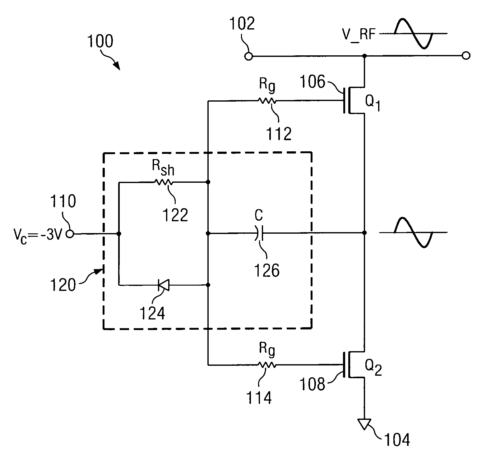
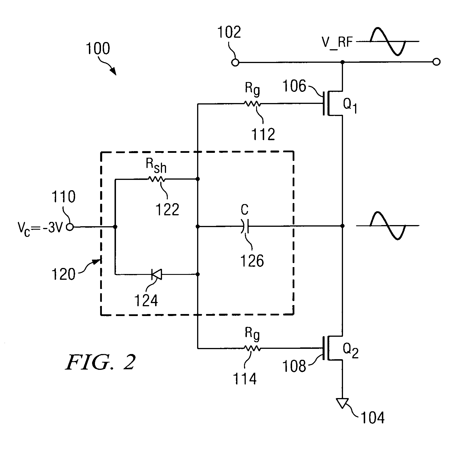
[0011] Example embodiments of the present invention and their advantages are best understood by referring to FIGS. 1 through 3B of the drawings, like numerals being used for like and corresponding parts of the various drawings.

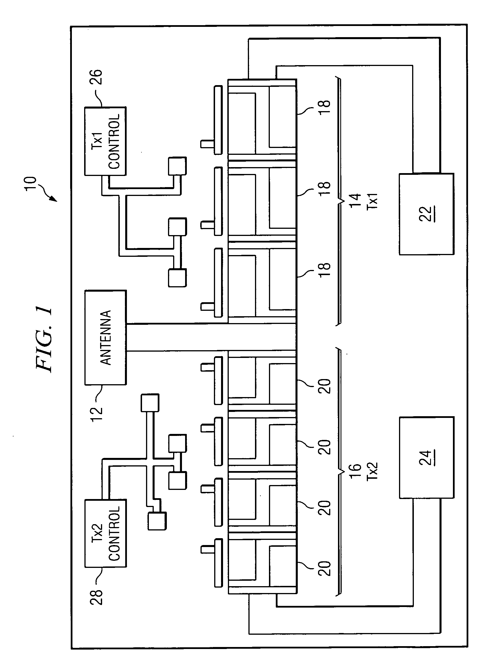
[0012]FIG. 1 is a schematic diagram illustrating a conventional high power switch 10. Switch 10 includes an antenna node 12, a first leg 14, a second leg 16, and output nodes 22 and 24. First leg 14 comprises a plurality of field effect transistors (FETs) 18 stacked in series. Second leg 16 includes a plurality of FETs 20 stacked in series.

[0013] In operation, a radio frequency, or alternating current, signal is received by antenna 12 and switched to output 22 or output 24. This switching is effected by either all FETs 18 or all FETs 20 in respective paths 14 and 16 turning on or off together. In some implementations, such as cellular phones, a control voltage for FETs 18 or 20, which may be applied at nodes 26 and 28 respectively, is conventionally −3 volts...


PUM


Abstract

According to one embodiment of the invention a method for switching an alternating current signal between at least two paths includes providing, in at least one of the paths, first and second field effect transistors in series. The method also includes providing a control voltage node operable to receive a control voltage and maintaining each of the first and second field effect transistors in pinch-off mode by offsetting a voltage on each gate of the field effect transistors with a DC voltage component other than the control voltage when it is desired for the alternating current not to flow through the at least one path.

Description

TECHNICAL FIELD OF THE INVENTION [0001] This invention relates generally to signal processing and more particularly to a method and system for high power switching. BACKGROUND OF THE INVENTION [0002] In terms of power handling a switch field effect transistor (FET) is limited in its high impedance “off”state by the gate bias voltage used to control the device. In the high impedance state, the switch FET is typically connected to an amplifier which is also biased off and has the effect of placing the switch FET in a shunt configuration with the source terminated in a short. As with most switch FETs, the gate terminal is terminated with an RF “open.” Thus, approximately half the RF voltage on the drain appears on the gate and is superposed on the gate bias voltage. The RF voltage swing on the switch FET turns the FET “on” for a portion of the RF cycle thereby reducing power handling if one of the following conditions occurs: (1) the RF voltage swing on the gate exceeds the pinch-off v...

Claims


Application Information

Patent Timeline
IPC IPC(8): G05F1/00
CPCH03K17/102H03K17/693H03K17/6871H03K17/10H03K17/687
Inventor HESTON, DAVID D.MOONEY, JON E.
Owner RAYTHEON CO
Learn More