Image sensor test apparatus

a technology of image sensor and test apparatus, which is applied in the direction of radio frequency control devices, instruments, television systems, etc., can solve the problems of insufficient size reduction of image sensor type apparatus, and achieve the effects of reducing the weight of the contact arms, preventing poor contact, and high speed movemen

Inactive Publication Date: 2007-07-12
ADVANTEST CORP
View PDF5 Cites 16 Cited by
  • Summary
  • Abstract
  • Description
  • Claims
  • Application Information

AI Technical Summary

Benefits of technology

[0007] The present invention relates to an image sensor test apparatus testing the optical characteristics of a CCD, CMOS, or other image sensor and has as its object the provision of an image sensor test apparatus enabling reduction of the size of the hardware.

Problems solved by technology

Therefore, with this image sensor test apparatus, space allowing provision of this fine adjustment mechanism and movement of the light source was required around the light source, thus the image sensor type apparatus could not be sufficiently reduced in size.

Method used


Image

  • Image sensor test apparatus
  • Image sensor test apparatus
  • Image sensor test apparatus

Examples


second embodiment

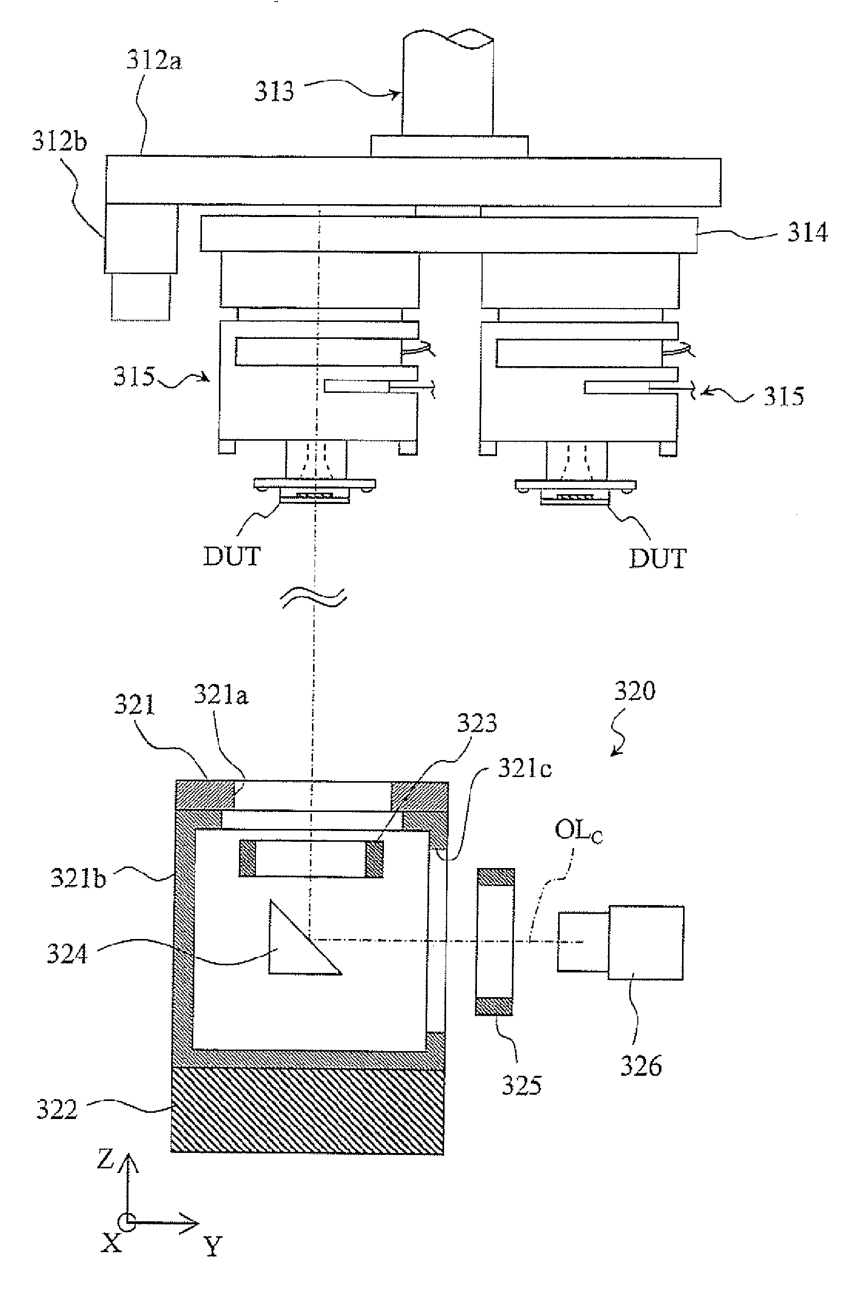
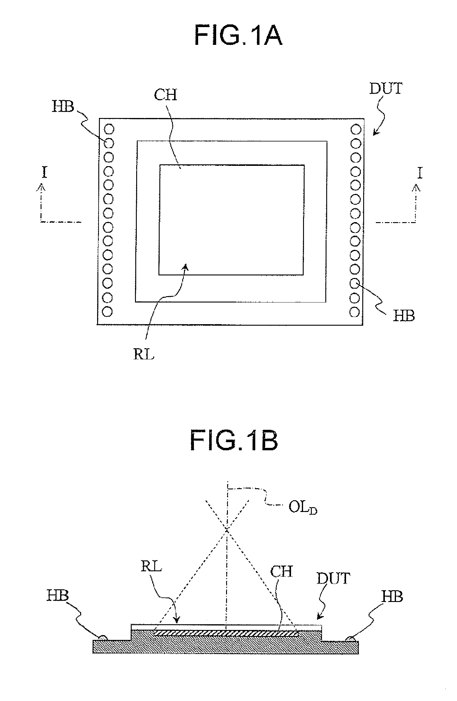
[0299]FIG. 34A is a top plan view showing an image sensor under test of an image sensor test apparatus according to a second embodiment of the present invention, FIG. 34B is a lower plan view of the image sensor shown in FIG. 34A, and FIG. 34C is a cross-sectional view of the image sensor along the VII-VII line of FIG. 34A, FIG. 35 is a schematic cross-sectional view showing contact arms and a test head of the image sensor test apparatus according to the second embodiment of the present invention, FIG. 30 is a schematic cross-sectional view showing the contact arms and alignment systems of the image sensor test apparatus according to the second embodiment of the present invention, FIG. 37 is an enlarged schematic cross-sectional view of an upper contact of a contact arm shown in FIG. 35 and FIG. 36, and FIG. 38 is a plan view of the upper contact shown in FIG. 37.

[0300] First, explaining the image sensors to be tested in the second embodiment of the present invention, this image se...


PUM


Abstract

An image sensor test apparatus that emits light to a light receiving surface of an image sensor (DUT) and inputs and outputs electrical signals from a contact part to input and output terminals of the image sensor so as to test the image sensor (DUT) for optical characteristics, which captures an image of the image sensor (DUT) in the state held by a contact arm (315) by a first camera (326), recognizes a relative position of the image sensor (DUT) with respect to the contact part by image processing, adds a precalculated amount of deviation of an optical axis of the image sensor (DUT) with respect to an optical axis of a light source to that relative position to calculate an amount of alignment of the image sensor (DUT), drives a drive unit (322) based on this, and moves a holding side arm (317) abutting against a movable stage (321) with a lock-and L-free mechanism (318) in a free state.

Description

TECHNICAL FIELD [0001] The present invention relates to an image sensor test apparatus bringing input and output terminals of a CCD, CMOS, or another image sensor into electrical contact wish a contact part of a test head, emitting light from a light source to the light receiving surface of the image sensor, and inputting and outputting electrical signals to and from the input and output terminals of the image sensor so as to test the optical characteristics of the image sensor. BACKGROUND ART [0002] An electronic device test apparatus referred to as a “handler” places a large number of semiconductor integrated circuit chips or other electronic devices on a tray, conveys the tray to the inside of the handler, brings each electronic device under test into electrical contact with the test head, and tests it at the electronic device test apparatus body (hereinafter referred to as a “tester). Further, when finishing this test, it ejects each electronic device from the test head and relo...

Claims


Application Information

Patent Timeline
Patent Type & Authority Applications(United States)
IPC IPC(8): H04N17/00G01M11/00G01R31/26H01L27/14H01L27/146
CPCG01M11/00H01L27/14618G01R31/2641H01L2224/16225H04N17/002H04N23/57
Inventor KIYOKAWA, TOSHIYUKI
Owner ADVANTEST CORP
Why Eureka
Try Eureka