Multi-chip package reducing peak power-up current

a technology of power-up current and multi-chips, applied in the direction of protective garments, instruments, goggles, etc., can solve the problems of increasing current consumption (and in particular peak current consumption), adverse effects of increasing current consumption

Inactive Publication Date: 2007-07-12
SAMSUNG ELECTRONICS CO LTD
View PDF3 Cites 82 Cited by
  • Summary
  • Abstract
  • Description
  • Claims
  • Application Information

AI Technical Summary

Problems solved by technology

While this capability is advantageous in some ways, it also tends to increase current consumption (and peak current consumption in particular) during power-up operations.
This increased current consumption has adverse implications to memory system specifications and related power supply sizing.

Method used


Image

  • Multi-chip package reducing peak power-up current
  • Multi-chip package reducing peak power-up current
  • Multi-chip package reducing peak power-up current

Examples


Embodiment Construction

[0013]The present invention will now be described in some additional detail with reference to the accompanying drawings in which several embodiments of the invention are shown. This invention may, however, be embodied in many different forms and should not be construed as being limited to only the embodiments set forth herein. Rather, these embodiments are presented as teaching examples. In the drawings, like numbers refer to like or similar elements.

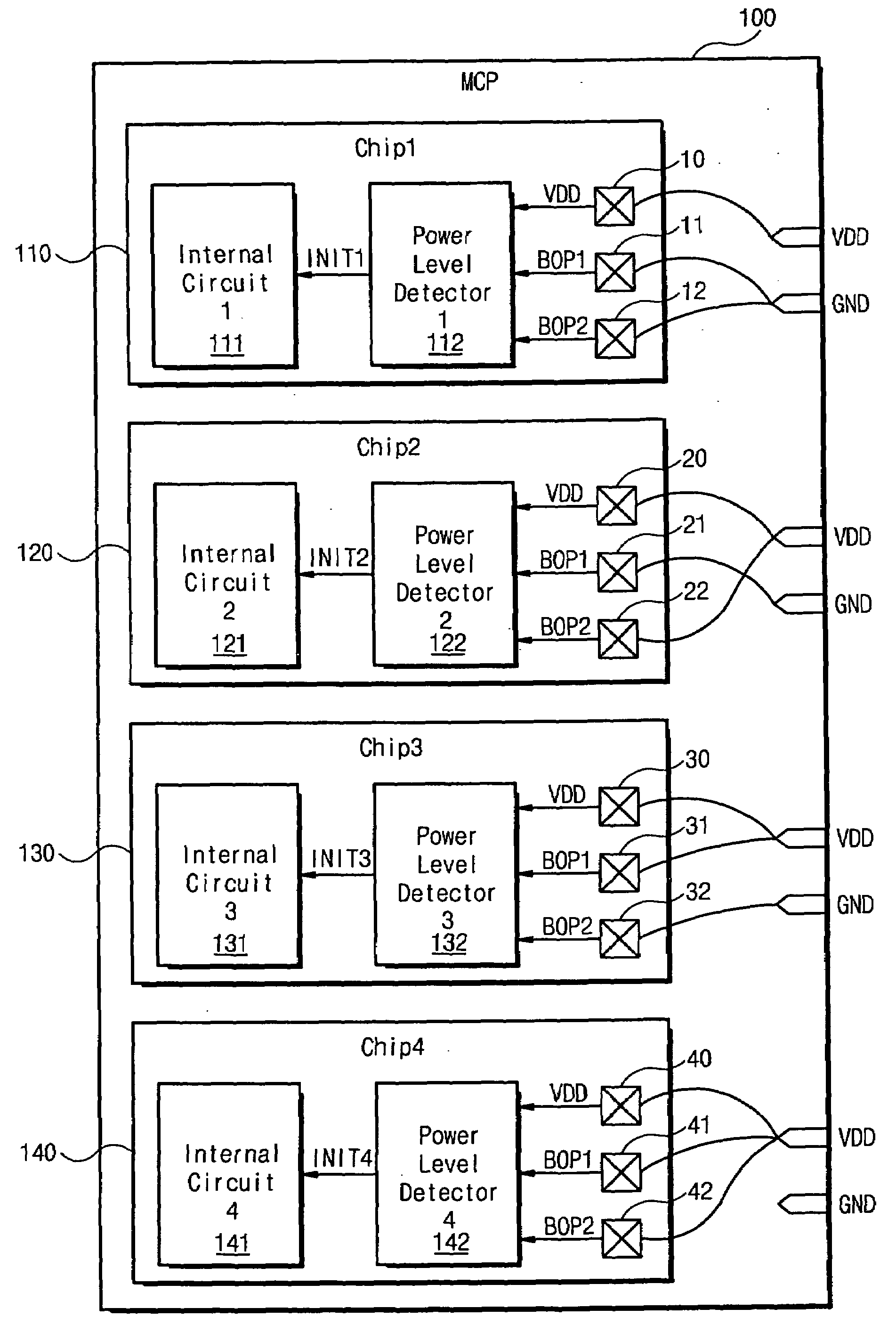
[0014]FIG. 1 shows a schematic block diagram of a multi-chip package (“MCP”) according to one embodiment of the invention. MCP 100 comprises a plurality of memory chips 110 through 140. Four (4) memory chips are used in the illustrated example, but those of ordinary skill in the art will recognize that any reasonable number of semiconductor chips, memory related or otherwise, might be used. Memory chips in a multi-chip package can be arranged in many manners. Further, the illustrated example of FIG. 1 shows a vertical arrangement (e.g.,...


PUM


Abstract

A multi-chip package is disclosed comprising a plurality of memory chips, each of the memory chips comprising an internal circuit; and a power level detector for detecting a level of a power supply voltage to initialize the internal circuit, at a power-up. The power level detectors in the respective memory chips are configured to initialize corresponding internal circuits at different points of time.

Description

BACKGROUND OF THE INVENTION[0001]1. Field of the Invention[0002]Embodiments of the invention relate to a multi-chip package and packaging technique. More particularly, embodiments of the invention relate to a multi-chip package comprising a plurality of memory chips.[0003]This application claims priority under 35 U.S.C § 119 to Korean Patent Application 2006-02297 filed on Jan. 9, 2006, the contents of which are hereby incorporated by reference.[0004]2. Description of Related Art[0005]Multi-chip packages are conventionally used to operationally group a plurality of semiconductor memory chips for use as a storage medium within electronic devices, such as computers. Semiconductor memory chips may be roughly divided between Random Access Memory (RAM) and Read Only Memory (ROM). ROM is commonly provided in the form of non-volatile memory devices capable of retaining stored data even when the power is turned off. ROM devices include programmable ROM (PROM), erasable PROM (EPROM), electri...

Claims


Application Information

Patent Timeline
Patent Type & Authority Applications(United States)
IPC IPC(8): G11C5/14
CPCG11C5/143G11C5/04A61F9/029A61F9/027G02C11/04A41D13/05G02C11/10
Inventor KWAK, PAN-SUK
Owner SAMSUNG ELECTRONICS CO LTD
Why Eureka
Try Eureka