Alignment plate

Inactive Publication Date: 2007-07-19
FUJITSU LTD
View PDF4 Cites 5 Cited by
  • Summary
  • Abstract
  • Description
  • Claims
  • Application Information

AI Technical Summary

Benefits of technology

[0031]With the present invention, an electronic component can be efficiently mounted on a printed circuit board, having an increased thickness, with adequate strength. Further, the electronic component can be mounted with adequate stren

Problems solved by technology

However, during such soldering step, the solder is often formed in inadequate statuses as shown in FIG. 4B and the through-holes are liable to be insufficiently filled with solder.
However, the related arts described above encounter issues described below.
Therefore, the electronic component 31 becomes hard to be firmly soldered onto the printed circuit board with the resultant difficulty in connecting the electronic component 31 to the printed circuit board with sufficient strength.
This results in

Method used


Image

  • Alignment plate
  • Alignment plate
  • Alignment plate

Examples


Embodiment Construction

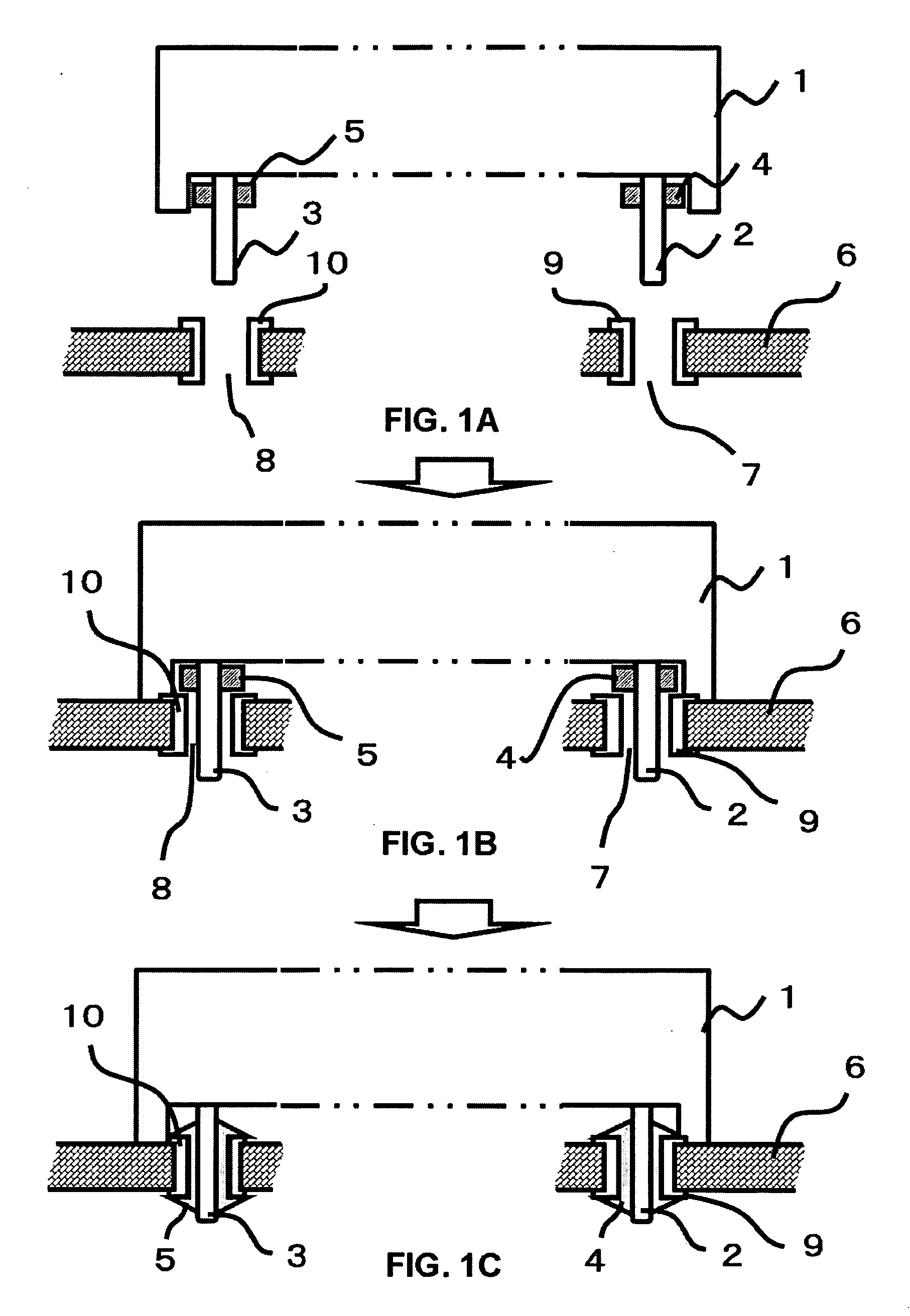
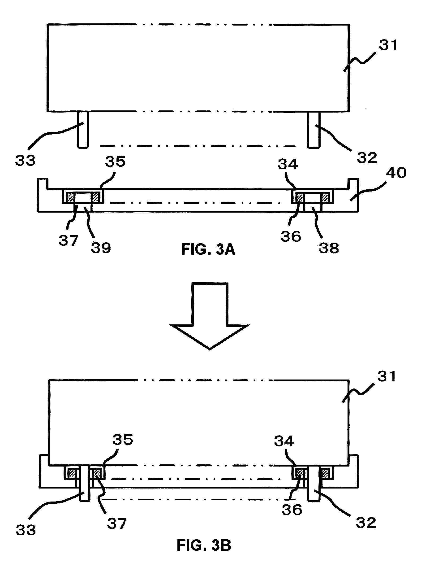
[0047]FIG. 6 is a cross-sectional view of a bracket of an embodiment according to an embodiment of the present invention.

[0048]With the present embodiment, the terminology “bracket” referred to a member used for mounting an electronic component on a printed circuit board and serves to locate solders onto the printed circuit board at areas in alignment with through-holes.

[0049]The electronic component 601 is placed on the bracket 602. Here, a surface of the bracket 602, on which the electronic component 601 is positioned, is referred to as an upper surface.

[0050]Further, the electronic component 601 has lead terminals 603, 604, 605. The lead terminals 603, 604, 605 are inserted to the through-holes of the printed circuit board and soldered thereto such that the electronic component 602 is mounted onto the printed circuit board.

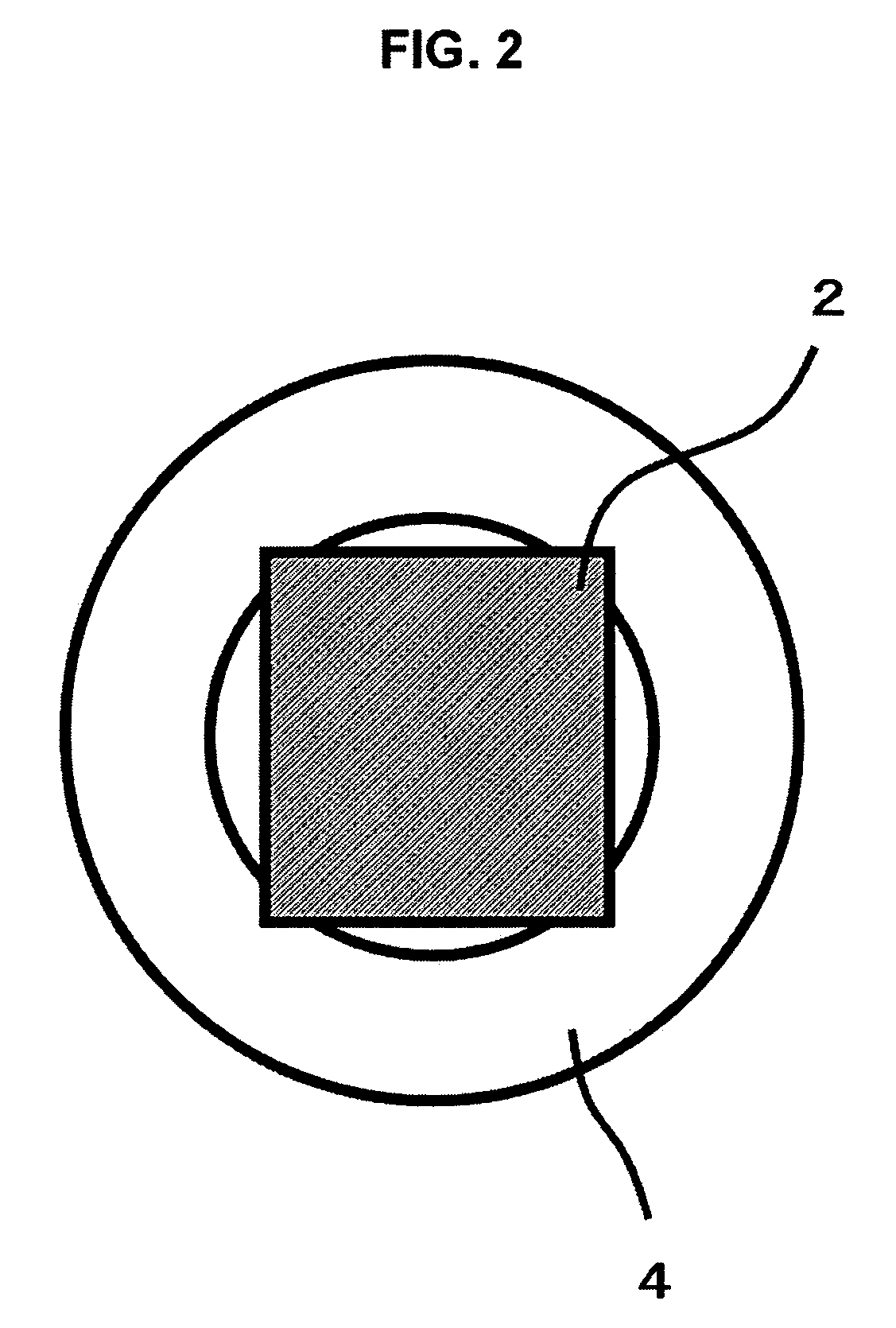
[0051]The upper surface of the bracket 602 is formed with dents 609, 610, 611 for placing solder rings 606, 607, 608 therein, respectively. With the present em...


PUM


Abstract

A mounting material alignment plate of the present invention is operative to place an electronic component to be mounted on a printed circuit board and has a plurality of bores that admit terminals of the electronic component to be placed. The mounting material alignment plate has first dents formed on one surface, on which the electronic component is located, around the individual bores, and second dents formed on another surface opposite to the one surface on which the electronic component is located.

Description

BACKGROUND OF THE INVENTION[0001]1. Field of the Invention[0002]The present invention relates to mounting component parts of printed substrates.[0003]2. Description of the Related Art[0004]In the related art, attempts have heretofore been made for mounting an electronic component onto a printed circuit board in mounting techniques listed below.[0005]FIGS. 1A to 1C are views showing the related art technology of mounting an electronic component onto a printed circuit board.[0006]FIGS. 1A to 1C are cross-sectional views of the electronic component 1 and the printed circuit board 6.[0007]In FIG. 1A, an electronic component 1 has lead terminals 2, 3 to which solder rings 4, 5 are press fitted in respective fixed places. In addition, as shown in FIG. 1B, the electronic component 1 is placed on the printed circuit board 6. When this takes place, the lead terminals 2, 3 of the electronic component 1 are inserted to through-holes 7, 8 formed in the printed circuit board 6. As shown in FIG. ...

Claims


Application Information

Patent Timeline
IPC IPC(8): A47J36/02
CPCH05K3/306H05K3/3447H05K3/3478H05K2201/10424H05K2203/176H05K2203/0113H05K2203/0271H05K2203/0415H05K2201/10984
Inventor SUEHIRO, MITSUO
Owner FUJITSU LTD
Why Eureka
Try Eureka