MOS transistor and method for forming the same

a technology of mos transistor and mos, which is applied in the direction of semiconductor devices, basic electric elements, electrical appliances, etc., can solve the problems of hindering the miniature tendency of a semiconductor device, deteriorating the uniformity of performance parameters of different devices, and difficulty in scaling down so as to reduce the equivalent oxide thickness, improve the device performance, and address the effect of deterioration of device performance uniformity

Active Publication Date: 2013-04-16
INST OF MICROELECTRONICS CHINESE ACAD OF SCI
View PDF8 Cites 3 Cited by
  • Summary
  • Abstract
  • Description
  • Claims
  • Application Information

AI Technical Summary

Benefits of technology

[0008]A technical problem solved by the invention is to effectively reduce equivalent oxide thickness, address deterioration of uniformity of device performance, and raise device performance.
[0056]Sacrificial metal spacers are formed on sidewalls of the gate stack to absorb oxygen of the gate stack, thereby obviating the problems in prior art, for example, increasing the equivalent oxide thickness and deteriorating uniformity of device performance. The sacrificial metal spacers have stress for promoting carrier mobility of MOS transistor and improving device performance.
[0057]Further, the invention is adapted for both gate-first process and gate-last process, and therefore facilitates process integration and promotes industrial applicability.

Problems solved by technology

And it is difficult to scale down the equivalent oxide thickness of the gate dielectric layer of the MOS transistor to 1 nm, in which high-k material is combined with a metal gate, hindering miniature tendency of a semiconductor device.
For instance, the oxygen in the interface oxide layer 10a is insufficient to convert the sacrificial metal layer 12b to an insulating metal oxide, resulting in different work function and equivalent oxide thickness of different devices, and correspondingly deteriorating uniformity of performance parameters, such as threshold voltage, of different devices.
The MOS transistor will not have stress by the above method, and thus the device performance, for instance carrier mobility, can not be raised.

Method used


Image

  • MOS transistor and method for forming the same
  • MOS transistor and method for forming the same
  • MOS transistor and method for forming the same

Examples


second embodiment

The Second Embodiment

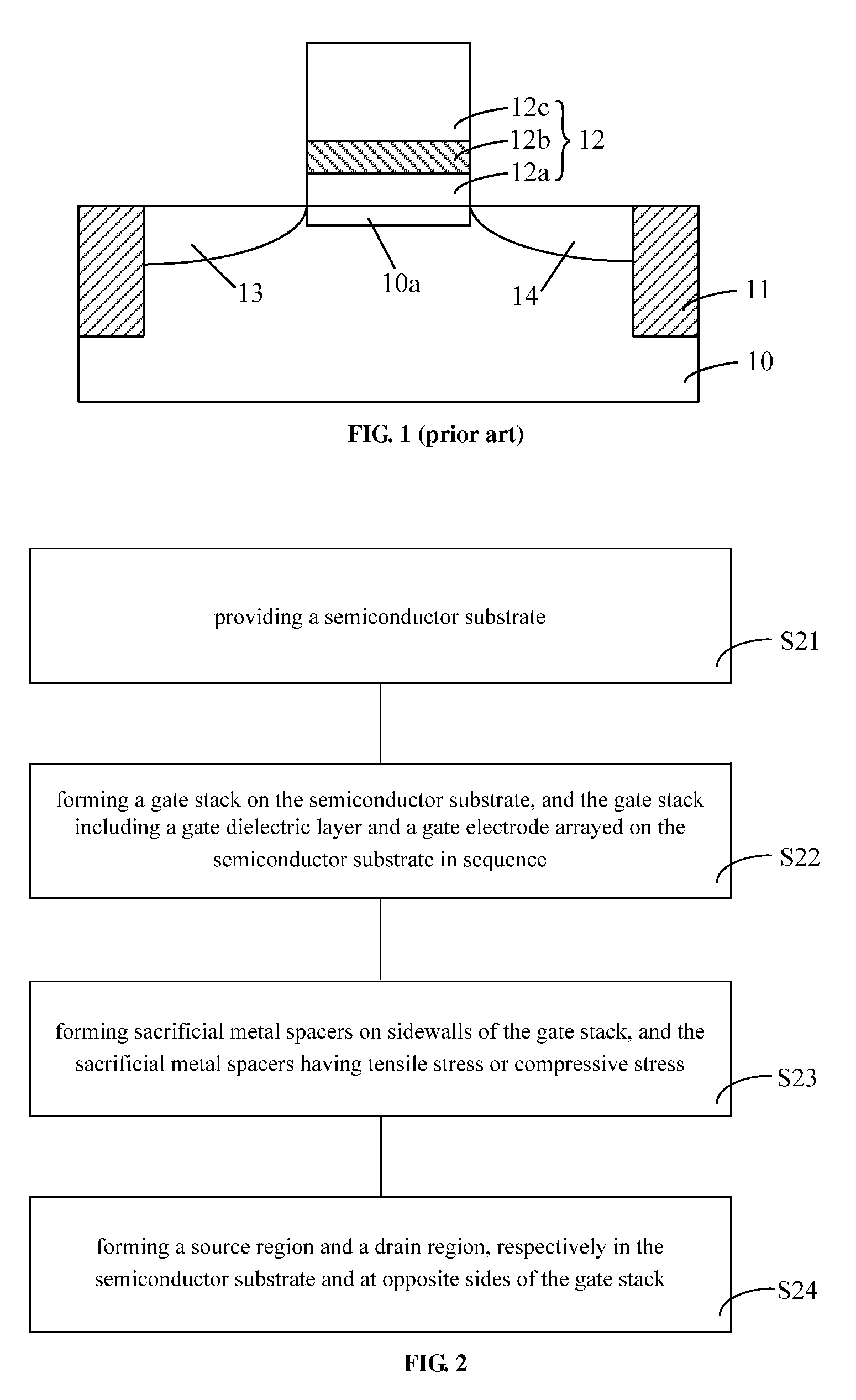
[0088]FIG. 10 is a schematic flow chart of the method for forming a MOS transistor according to the second embodiment of the present invention. A gate-last process is applied in the method of the second embodiment, as shown in FIG. 10. The method comprises:

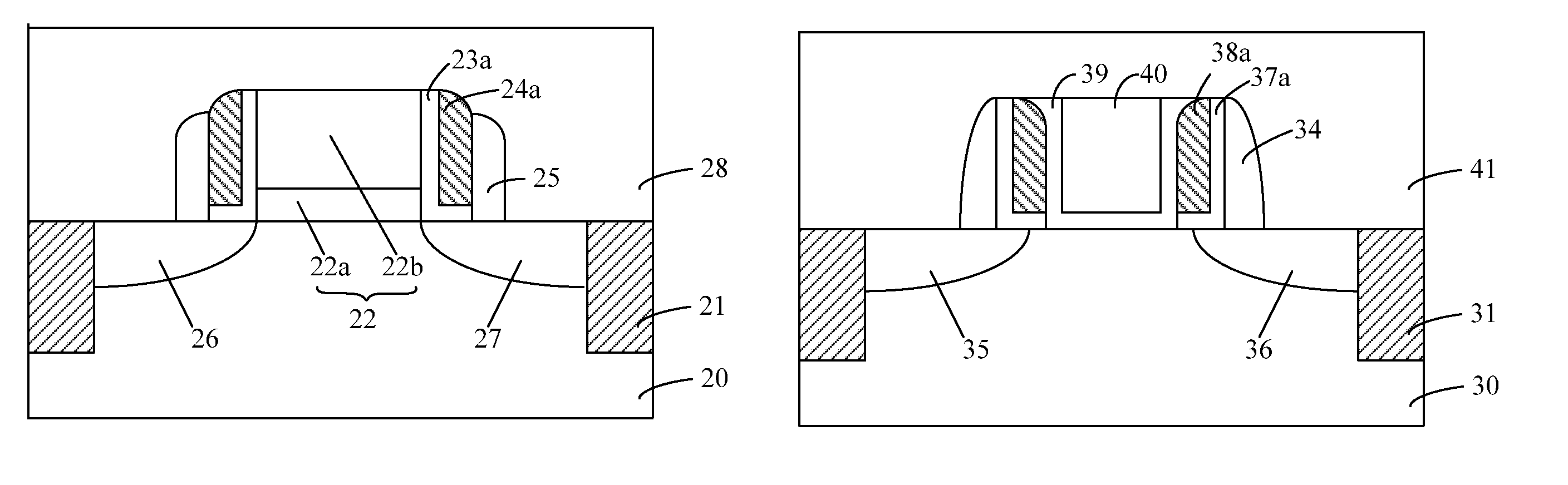
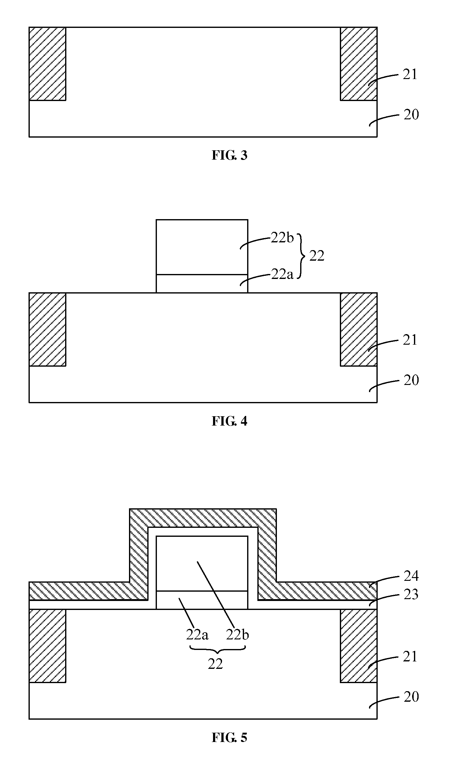
[0089]Step S31, providing a semiconductor substrate. A dielectric layer is formed on the semiconductor substrate, and defining an opening therein for exposing the semiconductor substrate. A source region and a drain region are respectively formed on the semiconductor substrate and at both sides of the opening.

[0090]Step S32, forming sacrificial metal spacers on both sides of the opening, the sacrificial metal spacers having tensile stress or compressive stress;

[0091]Step S33, forming a gate dielectric layer for covering the sacrificial metal spacers, and the semiconductor substrate which is exposed at the opening;

[0092]Step S24, filling a gate electrode in the opening.

[0093]FIGS. 11-16 are cross-sectional view...


PUM


Abstract

The invention provides a MOS transistor and a method for forming the MOS transistor. The MOS transistor includes a semiconductor substrate; a gate stack on the semiconductor substrate, and including a gate dielectric layer and a gate electrode on the semiconductor substrate in sequence; a source region and a drain region, respectively at sidewalls of the gate stack sidewalls of the gate stack and in the semiconductor; sacrificial metal spacers on sidewalls of the gate stack sidewalls of the gate stack, and having tensile stress or compressive stress. This invention scales down the equivalent oxide thickness, improves uniformity of device performance, raises carrier mobility and promotes device performance.

Description

CROSS REFERENCE TO RELATED APPLICATIONS[0001]The present application is a Section 371 National Stage Application of International Application No. PCT / CN2011 / 070695, filed on Jan. 27, 2011, which claims the benefit of CN 201010618284.2, filed on Dec. 31, 2010, the entire disclosure of which are incorporated herein by reference in their entirety.FIELD OF THE INVENTION[0002]The present invention relates to semiconductor device and semiconductor manufacture, and particularly to a MOS transistor and a method for forming the same.BACKGROUND OF THE INVENTION[0003]Manufacture process of MOS transistors typically comprises Gate-First process and Gate-Last process. A gate stack combines metal gate electrode, and gate dielectric layer of high-dielectric-constant (high-k) material which has a low Equivalent Oxide Thickness (EOT), and is widely employed at the technology node of 32 nm and beyond.[0004]An interface oxide layer, 4 Å or so in thickness, normally occurs between a gate dielectric lay...

Claims


Application Information

Patent Timeline
Patent Type & Authority Patents(United States)
IPC IPC(8): H01L21/336
CPCH01L29/4983H01L29/66545H01L29/78H01L29/6656H01L29/7845H01L29/66553
Inventor ZHONG, HUICAILIANG, QINGQINGYANG, DAZHAO, CHAO
Owner INST OF MICROELECTRONICS CHINESE ACAD OF SCI
Why Eureka
Try Eureka