Sequential access memory

a semiconductor memory and sequential access technology, applied in the direction of unauthorized memory use protection, digital storage, instruments, etc., can solve the problems of data corruption, data will be rewritten to an address that was not intended to be rewritten, and erroneous information will be recorded to the semiconductor memory device, so as to improve the reliability of data relating

Inactive Publication Date: 2007-07-19
SEIKO EPSON CORP
View PDF5 Cites 11 Cited by
  • Summary
  • Abstract
  • Description
  • Claims
  • Application Information

AI Technical Summary

Benefits of technology

[0004] The present invention is directed to addressing this problem, and has as an object to improve reliability o

Problems solved by technology

However, data corruption can occur, for example, during transfer of data input to a semiconductor memory device, and in such instances even if the data is rewritten normally to the semiconductor memory device, erroneous information will be recorded to the semiconductor memory device.
In the case of sequential access memory, since during accessing of a lower address accessing of dat

Method used


Image

  • Sequential access memory
  • Sequential access memory
  • Sequential access memory

Examples


Embodiment Construction

[0033] The memory device, write control method of data to the memory device, and printing device of the present invention will be described hereinbelow on the basis of certain preferred embodiments, making reference to the accompanying drawings.

Configuration of Semiconductor Memory Device

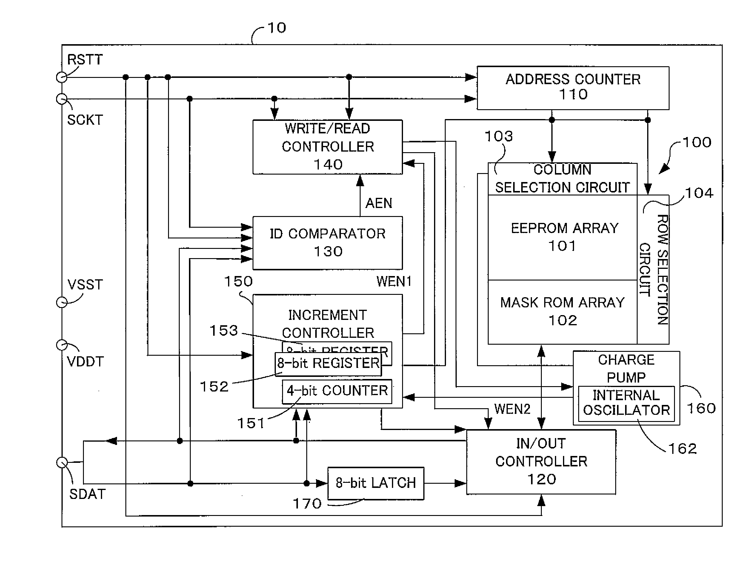
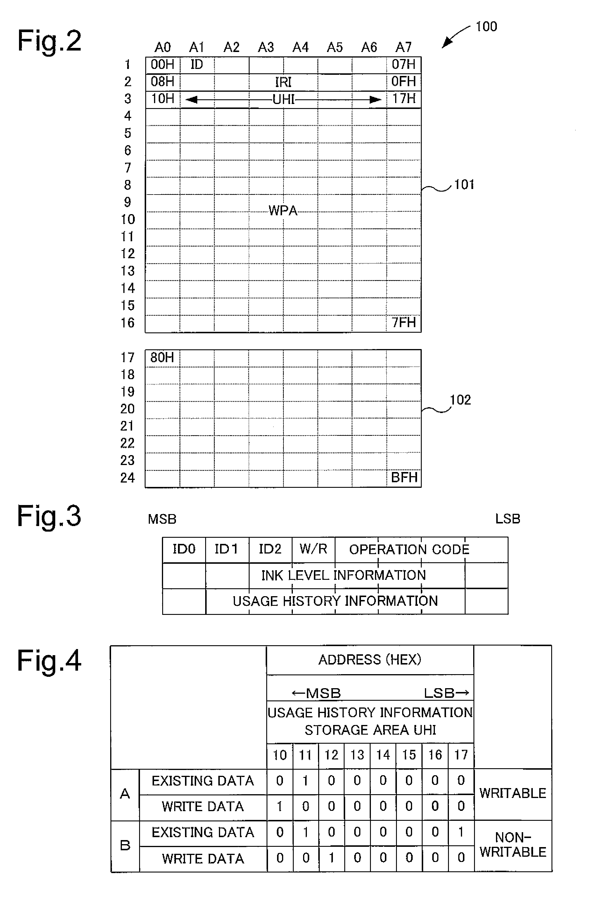
[0034] The configuration of the semiconductor memory device of the embodiment will be described with reference to FIGS. 1 and 2. FIG. 1 is a block diagram depicting the internal functional configuration of the semiconductor memory device according to an embodiment of the invention. FIG. 2 is an illustration depicting the format of an internal configuration map of a memory array provided to the semiconductor memory device according to the embodiment of the invention.

[0035] The semiconductor memory device 10 according to the present embodiment is a memory device of sequential access type that does not require input of address data specifying an access destination from the outside. The semiconducto...


PUM


Abstract

Semiconductor memory devices 10 are each furnished with a memory array 100 having an EEPROM array 101 and a mask ROM array 102. Identifying information for identifying each semiconductor memory device 10 is stored at the beginning three addresses of the EEPROM array 101. 8-bit data relating to ink level is stored at the ninth address to sixteenth address of the EEPROM array 101. The seventeenth address to the twenty-fourth address of the EEPROM array 101 is provided with a usage history information storage area for storing 8-bit usage history information that is rewriteable under certain conditions.

Description

BACKGROUND OF THE INVENTION [0001] The present invention relates to a sequentially-accessed semiconductor memory device, and to a print recording material receptacle furnished with a sequentially-accessed semiconductor memory device. [0002] Semiconductor memory devices, such as EEPROM for example, that permit only sequential access of data cells in a memory array are well known. Since such semiconductor memory devices are relatively inexpensive, they have come to be used as memory devices for holding information relating to receptacles containing consumable materials, for example. Data relating to usage history is a known example of information relating to receptacles containing consumable materials of this kind. While the nature of usage history data for a receptacle containing consumable material is to be updated in association with usage of the consumable material receptacle, in order for the usage history to be useful, there is a need to prevent to the usage history data from be...

Claims


Application Information

Patent Timeline
IPC IPC(8): G11C8/00G06F21/64G06F21/79
CPCG06F21/79G11C8/04G11C7/1006G06F2221/2101G11C16/02G06F12/14
Inventor ASAUCHI, NOBORU
Owner SEIKO EPSON CORP
Why Eureka
Try Eureka