Nonvolatile semiconductor storage device

Inactive Publication Date: 2007-07-26
KK TOSHIBA
View PDF6 Cites 23 Cited by
  • Summary
  • Abstract
  • Description
  • Claims
  • Application Information

AI Technical Summary

Benefits of technology

[0011]The first aspect of the present invention is a nonvolatile semiconductor storage device comprising a plurality of juxtaposed NAND strings, each of the plurality of NAND strings comprising: a memory cell block obtained by connecting current paths of a plurality of nonvolatile memory cells in series, each of the plurality of nonvolatile memory cells comprising a floating gate electrode formed on a first insulating film on a device area isolated by an isolation insulating film which forms an isolation in a semiconductor substrate, and a control gate electrode formed on a second insulating film on the floating gate electrode to cover side surfaces and an upper surface of the floating gate electrode; a first selection gate transistor comprising a first gate electrode in which a first electrode layer made of the same electrode material as the floating gate electrode and a second electrode layer made of the same electrode material as the control gate electrode are formed in direct contact with each other through a first hole formed in a portion of a third insulating film made of the same insulating material as the second insulating film, a current path of the first selection gate transistor comprising one end connected to one end of current paths of series-connected nonvolatile memory cells in the memory cell block, and the other end connected to a data transfer line v

Problems solved by technology

Accordingly, a large leakage current or low breakdown voltage of the control g

Method used


Image

  • Nonvolatile semiconductor storage device
  • Nonvolatile semiconductor storage device
  • Nonvolatile semiconductor storage device

Examples


first embodiment

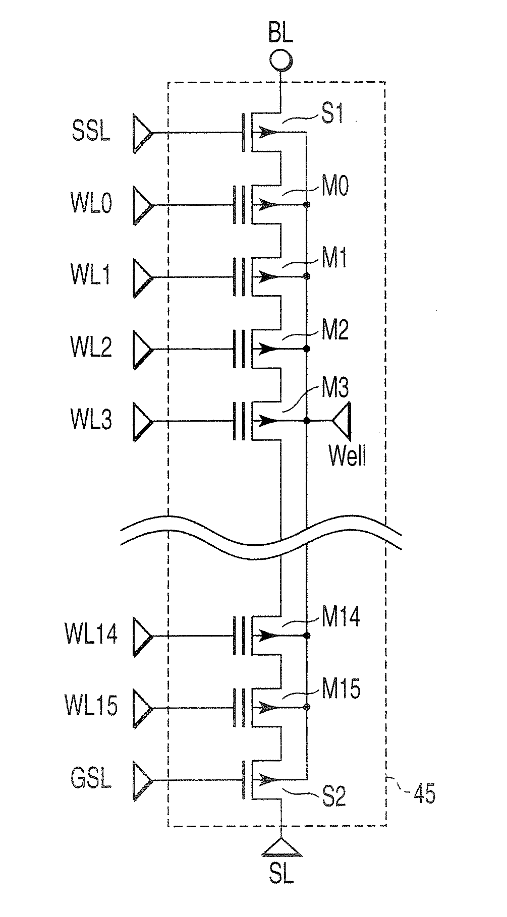
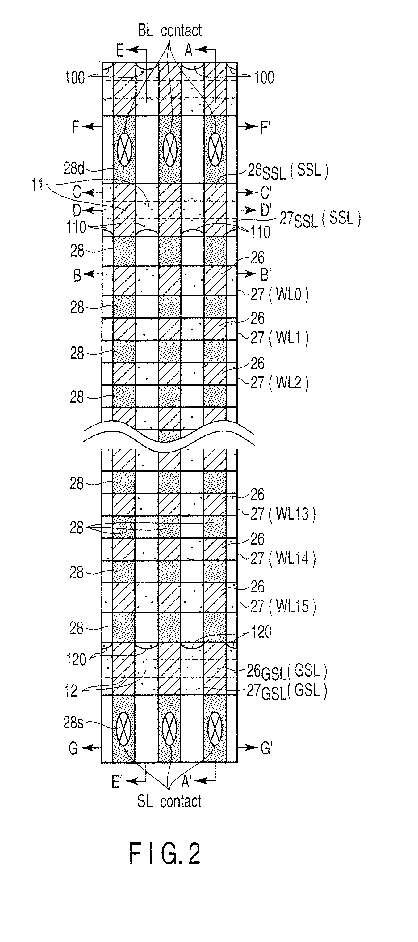
[0072]FIGS. 1 and 2 illustrate the structure of a nonvolatile semiconductor storage device according to the first embodiment of the present invention. In these figures, the suffixes of symbols represent the differences between the positions of elements used, and elements having the same main symbol indicate parts formed in the same step by using the same material.

[0073]FIG. 1 is an equivalent circuit diagram of a NAND string 45. FIG. 2 is a plan view of the layout of a plurality of juxtaposed NAND strings. FIG. 2 shows a structure obtained by juxtaposing three NAND strings shown in FIG. 1. FIG. 2 shows only a structure below control gate electrodes 27 in order to clearly indicate the structures of a memory cell and selection gate transistor.

[0074]As shown in FIG. 1, the current paths of nonvolatile memory cells M0 to M15 comprising MOS transistors each having a floating gate electrode (charge storage electrode) 26 connect in series to form a NAND memory cell block. One end of the se...

second embodiment

[0137]FIG. 18 is a plan view of the layout of a nonvolatile semiconductor storage device according to the second embodiment of the present invention. Note that in the following description, the same reference numerals as in FIG. 2 denote the same parts, and a detailed explanation thereof will be omitted. Note also that the suffixes of symbols represent the differences between the positions of elements used, and elements having the same main symbol indicate parts formed in the same step by using the same material.

[0138]FIG. 18 shows a structure obtained by juxtaposing three NAND strings shown in the equivalent circuit diagram of FIG. 1. FIG. 18 shows only a structure below gate electrodes 27 in order to clearly indicate the cell structure. Referring to FIG. 18, nonvolatile memory cells M0 to M15 comprising MOS transistors each having a floating gate electrode 26 connect in series, and one end connects to a data transfer line via a selection transistor S1. The other end connects to a ...

third embodiment

[0151]FIG. 26 is a plan view of the layout of a nonvolatile semiconductor storage device according to the third embodiment of the present invention. Note that the same reference numerals as in the nonvolatile semiconductor storage devices according to the first and second embodiments denote the same parts, and a detailed explanation thereof will be omitted. Note also that the suffixes of symbols represent the differences between the positions of elements used, and elements having the same main symbol indicate parts formed in the same step by using the same material.

[0152]FIG. 26 shows a structure obtained by juxtaposing three NAND strings shown in the equivalent circuit diagram of FIG. 1. FIG. 26 particularly shows only a structure below control gate electrodes 27 in order to clearly indicate the cell structure. Referring to FIG. 26, nonvolatile memory cells M0 to M15 comprising MOS transistors each having a floating gate electrode 26 connect in series, and one end connects to a dat...


PUM


Abstract

In a nonvolatile semiconductor storage device having a plurality of NAND strings, each NAND string includes a memory cell block obtained by connecting a plurality of nonvolatile memory cells in series, a first selection gate transistor connected to a data transfer line contact, and a second selection gate transistor connected to a source line contact. The upper surface of an isolation insulating film between adjacent data transfer line contacts is higher than the major surface of a semiconductor substrate in a device area between the first selection gate transistor and data transfer line contact. Alternatively, the upper surface of an isolation insulating film between adjacent source line contacts is higher than the major surface of the semiconductor substrate in a device area between the second selection gate transistor and source line contact.

Description

CROSS-REFERENCE TO RELATED APPLICATIONS[0001]This application is based upon and claims the benefit of priority from prior Japanese Patent Applications No. 2006-013761, filed Jan. 23, 2006; and No. 2006-140327, filed May 19, 2006, the entire contents of both of which are incorporated herein by reference.BACKGROUND OF THE INVENTION[0002]1. Field of the Invention[0003]The present invention relates to a nonvolatile semiconductor storage device which includes a plurality of memory cell blocks comprising nonvolatile semiconductor storage elements each having a floating gate electrode, and selects a memory cell block by a selection gate transistor.[0004]2. Description of the Related Art[0005]A memory cell of an EEPROM generally has a MISFET structure formed by stacking a floating gate electrode (charge storage layer) and control gate electrode on a semiconductor substrate. This nonvolatile memory cell transistor stores data by using the difference between a threshold value in a state in wh...

Claims


Application Information

Patent Timeline
IPC IPC(8): G11C16/04
CPCG11C16/0483H01L27/11524H01L27/11521H01L27/115H10B69/00H10B41/30H10B41/35A01K97/06A01K91/047
Inventor NOGUCHI, MITSUHIRO
Owner KK TOSHIBA
Why Eureka
Try Eureka