Self-aligned trench MOSFET structure and method of manufacture

a technology of mosfet and self-alignment, which is applied in the direction of basic electric elements, electrical apparatus, and semiconductor devices. it can solve the problems of increasing manufacturing costs, limiting factors to higher current ratings is the breakdown voltage, and increasing costs

Active Publication Date: 2007-07-26
SEMICON COMPONENTS IND LLC
View PDF10 Cites 43 Cited by
  • Summary
  • Abstract
  • Description
  • Claims
  • Application Information

AI Technical Summary

Problems solved by technology

As the complexity and sophistication of power devices increases, the number of process steps and masks in the manufacturing process also increases, significantly increasing the manufacturing costs.
One of the limiting factors to higher current ratings is the breakdown voltage, particularly in the edge termination region where array junctions terminate.
However, termination structures (particularly the planar field plate variety) occupy relatively large areas of the die and require additional masking and processing steps, thus resulting in increased costs.

Method used


Image

  • Self-aligned trench MOSFET structure and method of manufacture
  • Self-aligned trench MOSFET structure and method of manufacture
  • Self-aligned trench MOSFET structure and method of manufacture

Examples


Embodiment Construction

[0015] The present invention relates generally to semiconductor power device technology, and more particularly to improved power devices with enhanced termination structures, and methods of forming the same.

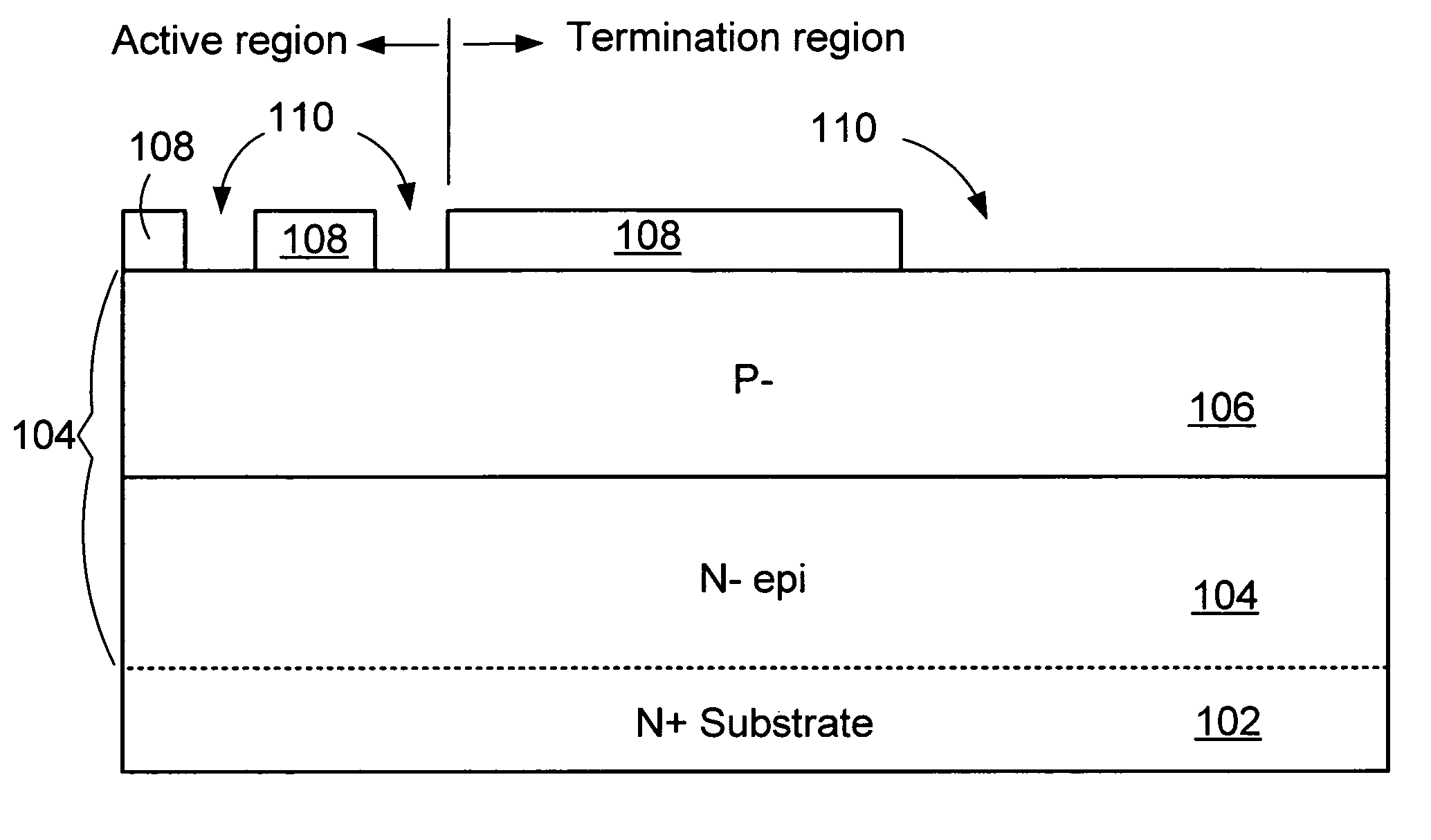
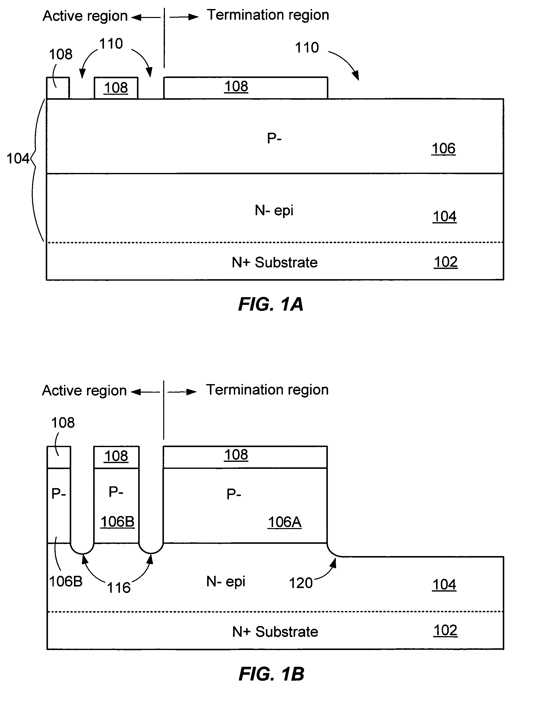
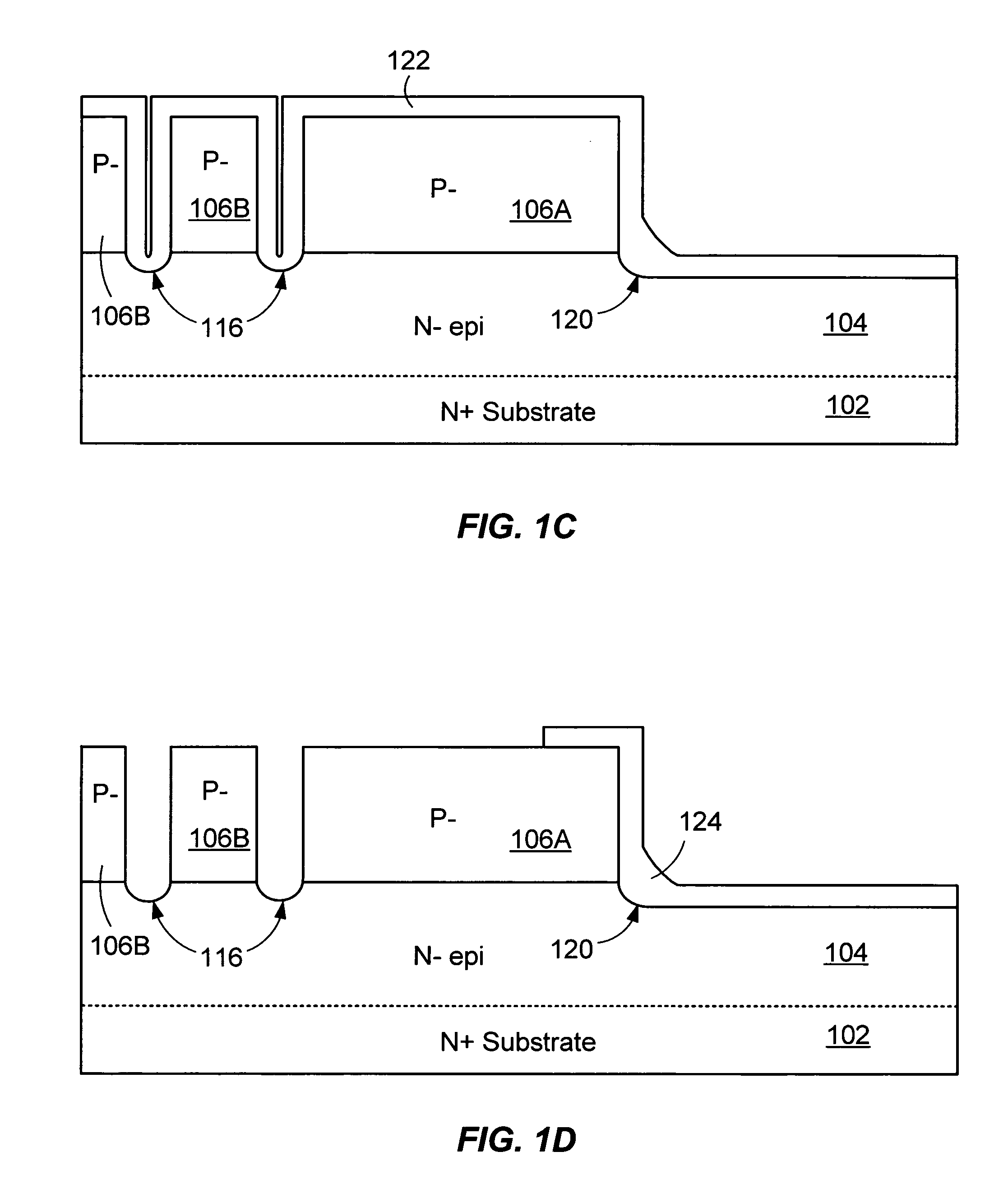
[0016]FIGS. 1A-1K are simplified cross-section views at various steps of a manufacturing process for forming a self-aligned MOSFET with a trench field plate termination structure, in accordance with an exemplary embodiment of the invention. FIG. 2 is a simplified cross-section view showing a trench gate runner structure formed without requiring additional processing steps to those depicted by FIGS. 1A-1K. All drawings described herein are merely illustrative and thus are not intended to unduly limit the scope of the claims herein. One of ordinary skill in the art would recognize many possible variations, modifications, and alternatives in view of this disclosure.

[0017] In FIG. 1A, a lightly doped N-type epitaxial layer 104 is formed over a highly doped N-type substrate using co...


PUM


Abstract

PATENT A trench gate FET is formed as follows. A well region is formed in a silicon region. A plurality of active gate trenches and a termination trench are simultaneously formed in an active region and a termination region of the FET, respectively, such that the well region is divided into a plurality of active body regions and a termination body region. Using a mask, openings are formed over the termination body region and the active body region. Dopants are implanted into the active body regions and the termination body region through the openings thereby forming a first region in each active and termination body region. Exposed surfaces of all first regions are recessed so as to form a bowl-shaped recess having slanted walls and a bottom protruding through the first region such that remaining portions of the first region in each active body region form source regions that are self-aligned to the active gate trenches.

Description

CROSS-REFERENCES TO RELATED APPLICATIONS [0001] This application relates to the patent application Ser. No. 11 / 317,653, titled “Trench Field Plate Termination For Power Devices,” filed Dec. 22, 2005, incorporated herein by reference in its entirety for all purposes.BACKGROUND OF THE INVENTION [0002] There continues to be a growing demand for semiconductor power devices (i.e., devices capable of carrying large currents at high voltages). Such devices include bipolar transistors, insulated gate bipolar transistors (IGBT), metal oxide semiconductor field effect transistors (MOSFET) and other types of field effect transistors. Notwithstanding significant advances in power device technology, there remains a need for still higher-performing and more cost-effective devices. As the complexity and sophistication of power devices increases, the number of process steps and masks in the manufacturing process also increases, significantly increasing the manufacturing costs. Thus, processing tech...

Claims


Application Information

Patent Timeline
Patent Type & Authority Applications(United States)
IPC IPC(8): H01L21/336
CPCH01L29/407H01L29/41766H01L29/42368H01L29/66727H01L29/0661H01L29/7811H01L29/7813H01L29/4236H01L29/66734H01L21/18
Inventor KOCON, CHRISTOPHER BOGUSLAWKRAFT, NATHAN LAWRENCE
Owner SEMICON COMPONENTS IND LLC
Why Eureka
Try Eureka