Apparatus and method for inspecting defects

a technology of apparatus and defects, applied in the direction of optical investigation of flaws/contamination, semiconductor/solid-state device testing/measurement, instruments, etc., can solve the problems of insufficient consideration of a design capable of inspecting very small particle-like contamination, scratching, and other defects, and achieves a high-efficiency manufacturing line for substrates

Inactive Publication Date: 2007-08-02
HITACHI HIGH-TECH CORP
View PDF7 Cites 35 Cited by
  • Summary
  • Abstract
  • Description
  • Claims
  • Application Information

AI Technical Summary

Benefits of technology

[0006] The present invention also provides an apparatus and method for inspecting defects, adapted such that a highly efficient manufacturing line for substrates can be constructed by using the apparatus as an in-line monitor.

Problems solved by technology

In Patent Documents 1-7 outlined above, however, sufficient consideration has not been paid to a design capable of inspecting very small particle-like contamination, thin-film-like contamination, scratches, and other defects present on various types of substrates that is to be inspected, in a simple configuration.

Method used


Image

  • Apparatus and method for inspecting defects
  • Apparatus and method for inspecting defects
  • Apparatus and method for inspecting defects

Examples


Embodiment Construction

[0064] Hereunder, embodiments of the present invention will be described using the accompanying drawings.

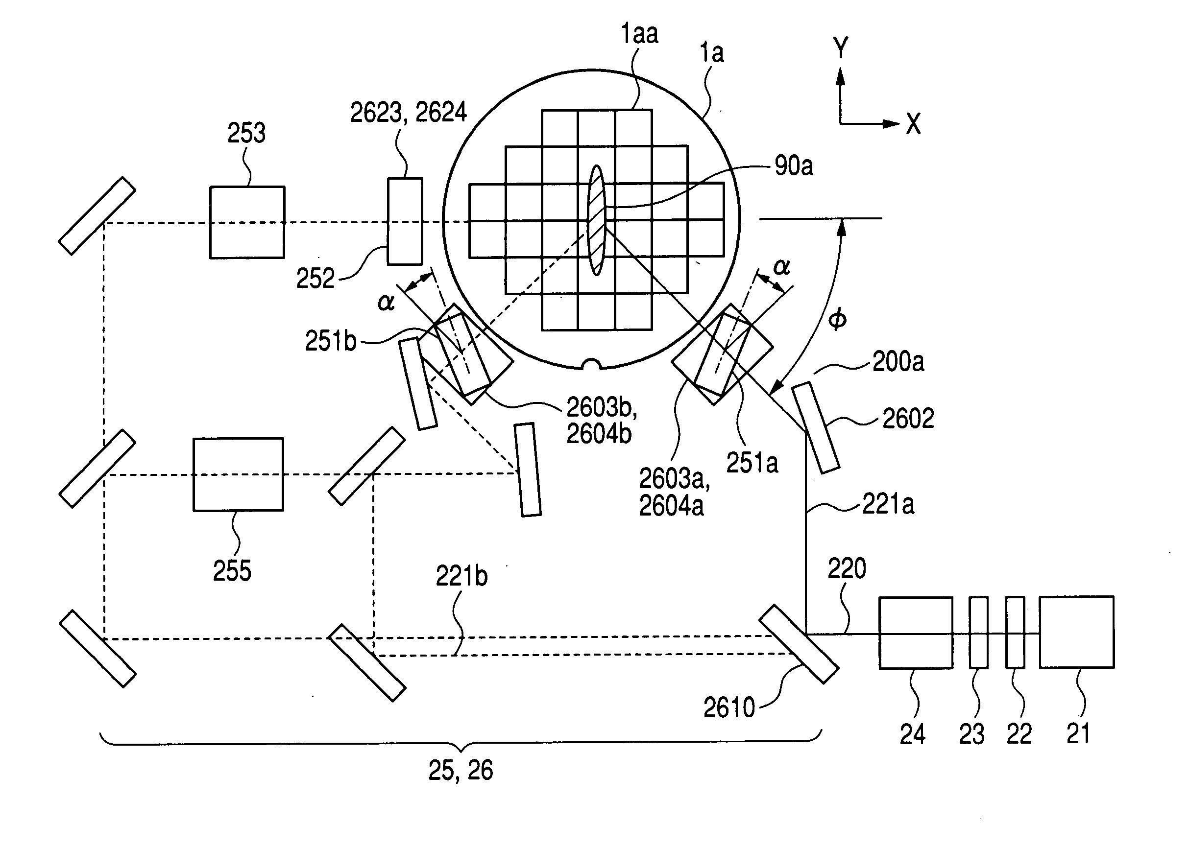
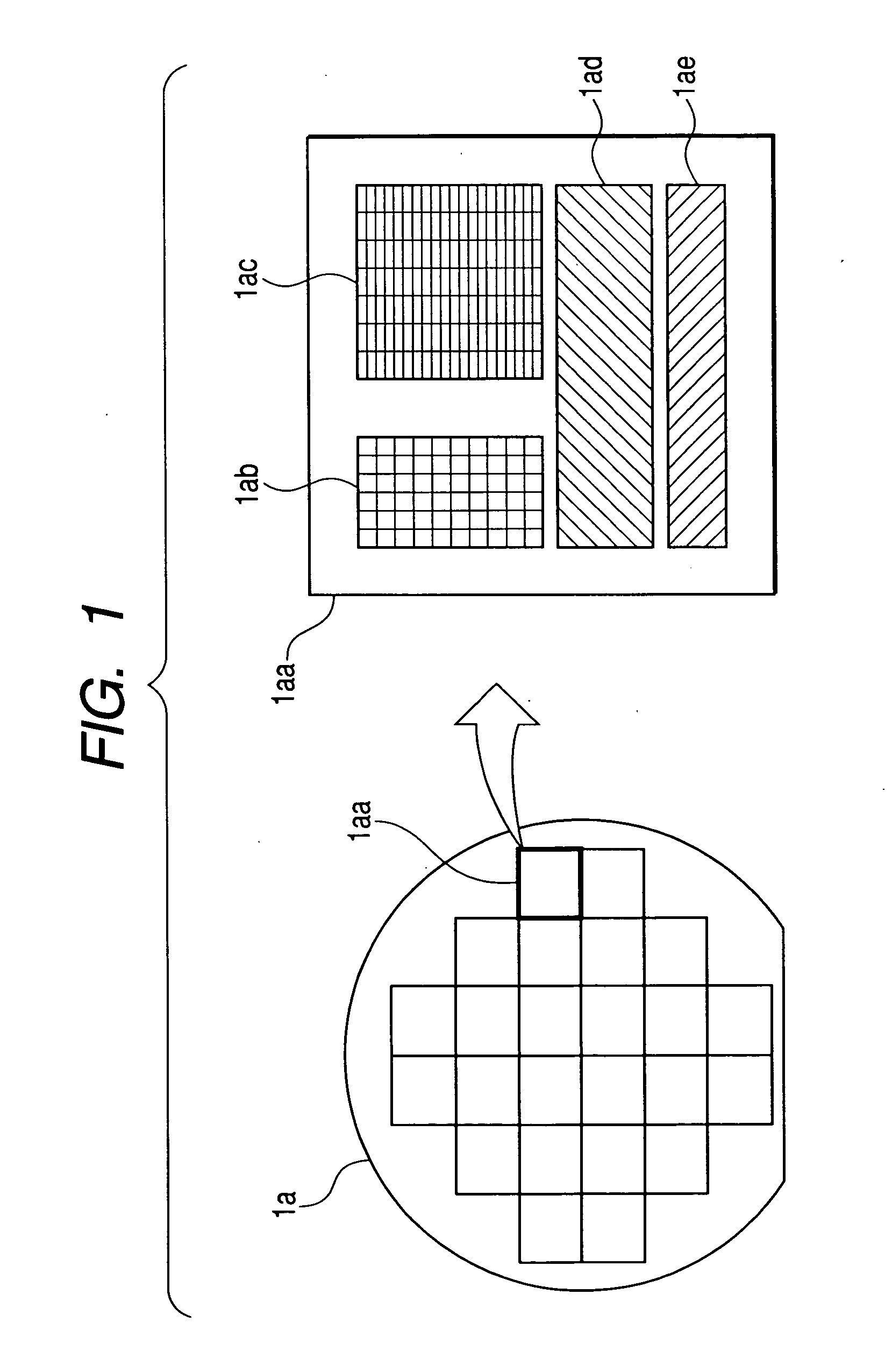
[0065] One possible kind of object 1 to be subjected to inspection of defects such as contamination, is a semiconductor wafer “1a” with chips “1aa” arrayed two-dimensionally at required spatial intervals (hereinafter, the object 1 is referred to as the inspection target 1). An interior of each chip “1aa” is mainly formed up by a register group region “1ab”, a memory region “1ac”, a CPU core region “1ad”, and an input / output region “1ae”. The register group region “1ab” and the memory region “1ac” are both formed by two-dimensionally and regularly arranging patterns with a minimum line width ranging from about 0.05 to 0.02 μm. The CPU core region “1ad” and the input / output region “1ae” are both formed by non-iteration of patterns with a minimum line width ranging from about 0.05 to 0.02 μm. In this way, even when the inspection target 1 for the inspection of contamination and oth...


PUM

PropertyMeasurementUnit
widthaaaaaaaaaa
sizeaaaaaaaaaa
wavelengthaaaaaaaaaa

Abstract

A defect inspection apparatus includes an irradiation optical system 20, a detection optical system 30, and an image processor 40. In the irradiation optical system, a mirror 2603 is disposed to reflect downward a beam flux that has been guided to a first or second optical path, and a cylindrical lens 251 and an inclined mirror 2604 are disposed to focus the beam flux that has been directed downward by the mirror, at an inclination angle from a required oblique direction extending horizontally, onto a substrate 1 to be inspected, as a slit-shaped beam 90.

Description

BACKGROUND OF THE INVENTION [0001] The present invention relates to an apparatus and method for inspecting defects, adapted to detect and analyze contamination and other defects occurring during the manufacturing processes of a desired object that include forming patterns on a substrate, to provide appropriate measures against contamination and other defects, and to inspect the occurrence status thereof. The manufacturing processes include semiconductor manufacturing processes, liquid-crystal display device manufacturing processes, printed-circuit board manufacturing processes, and the like. [0002] During conventional semiconductor-manufacturing processes, the presence of dust particles or other foreign substances (hereinafter, referred to collectively as contamination) on the surface of a semiconductor substrate (wafer) causes defects such as the improper insulation or short-circuiting of wiring. In addition, if a semiconductor device becomes fine-structured to form fine-structured...

Claims


Application Information

Patent Timeline
Patent Type & Authority Applications(United States)
IPC IPC(8): G01N21/88
CPCG01N21/94G01N21/9501G01N21/95607H01L22/12G01N2021/9513G01N2021/95638G01N21/95623
Inventor NAKANO, HIROYUKIHAMAMATSU, AKIRAUTO, SACHIOOSHIMA, YOSHIMASANISHIYAMA, HIDETOSHIURANO, YUTAMAEDA, SHUNJI
Owner HITACHI HIGH-TECH CORP
Why Eureka
Try Eureka