Triple-well CMOS devices with increased latch-up immunity and methods of fabricating same

a technology of triple-well cmos and latch-up immunity, which is applied in the direction of semiconductor devices, electrical equipment, transistors, etc., can solve the problems of catastrophic failure of devices in which it occurs and even regions of integrated circuit chips, and achieve the effect of reducing latch-up

Inactive Publication Date: 2007-08-02
INT BUSINESS MASCH CORP
View PDF3 Cites 23 Cited by
  • Summary
  • Abstract
  • Description
  • Claims
  • Application Information

AI Technical Summary

Benefits of technology

[0006] A third aspect of the present invention is a method of reducing latch-up in a CMOS device comprising: forming an N-well and an adjacent P-well in a silicon substrate; forming a PFET and a N-type contact in the N-well, forming an NFET and a P-type contact in the P-well; forming a buried N-type doped layer in the P-well, the CMOS device including a parasitic bipolar NPN transistor, an emitter of the parasitic bipolar NPN transistor comprising a source of the NFET, a base of the parasitic bipolar NPN transistor comprising a region of the P-well under the NFET, and a collector of the parasitic bipolar NPN transistor comprising the buried N-type doped layer and the N-well; and increasing a latch-up holding voltage of the CMOS device above a power supply voltage level supplied to the CMOS device by channeling holes around the bipolar NPN transistor parasitic transistor and into the P-well contact

Problems solved by technology

However, the combination of lightly P-type doped substrates and triple well structures includes parasitic NPN and PNP bipolar transistors in adjacent NFETs and PFETs which can form a parasitic latch and can go into latch-up mode (high current flow with feedback) when charge pairs are generated, for example, by heavy ions striking the sources, drains or wells of adjacent NFETs and PFETs or by unanticipated voltage variations in the power supplies feeding the sources, drains or wells of adjacent NFETs and PFETs.
Latch-up, when it occurs, can result in catastrophic failure of the devices in which it occurs and even regions of the integrated circuit chip containing the latched-up devices.

Method used


Image

  • Triple-well CMOS devices with increased latch-up immunity and methods of fabricating same
  • Triple-well CMOS devices with increased latch-up immunity and methods of fabricating same
  • Triple-well CMOS devices with increased latch-up immunity and methods of fabricating same

Examples


Embodiment Construction

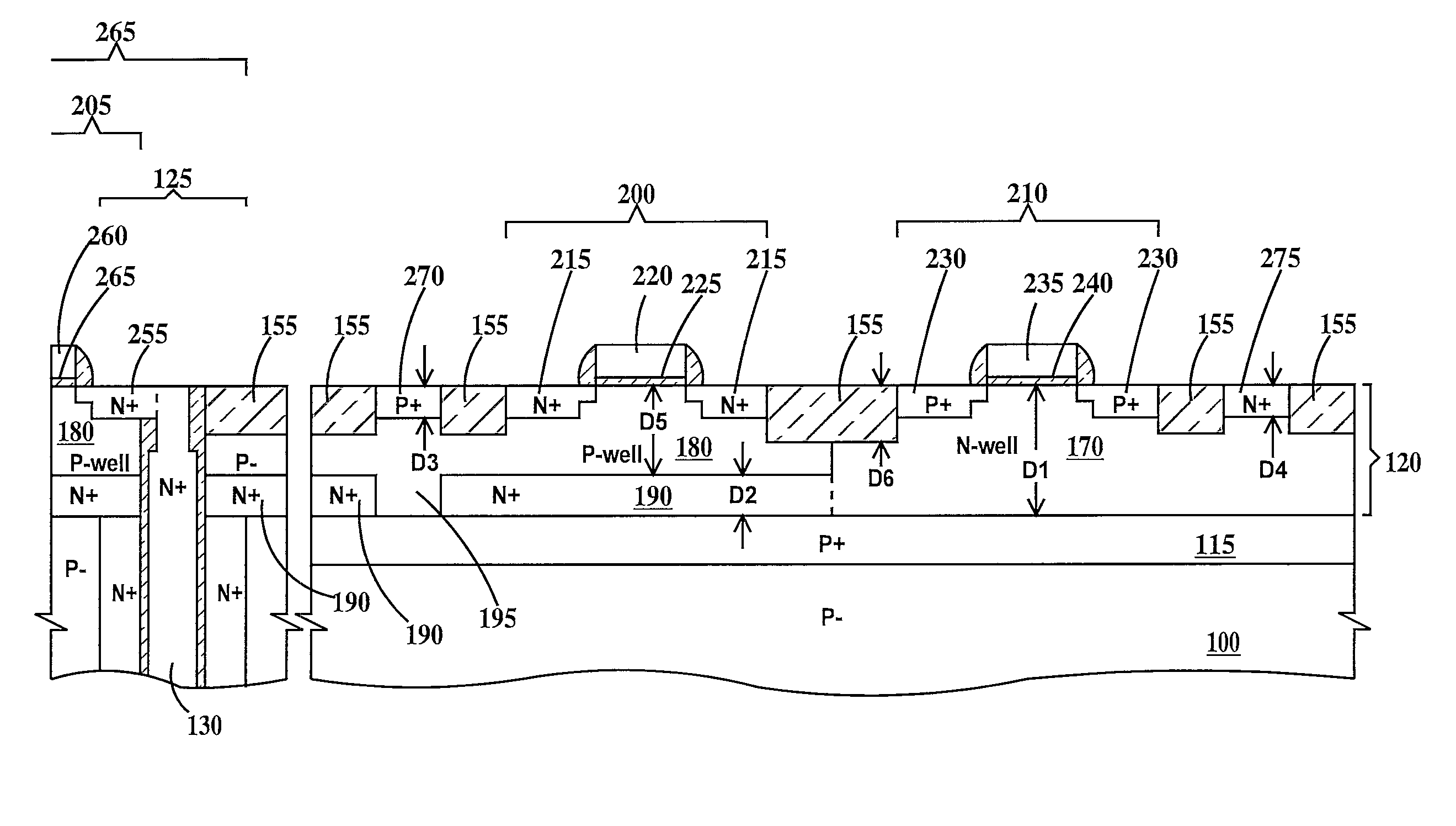
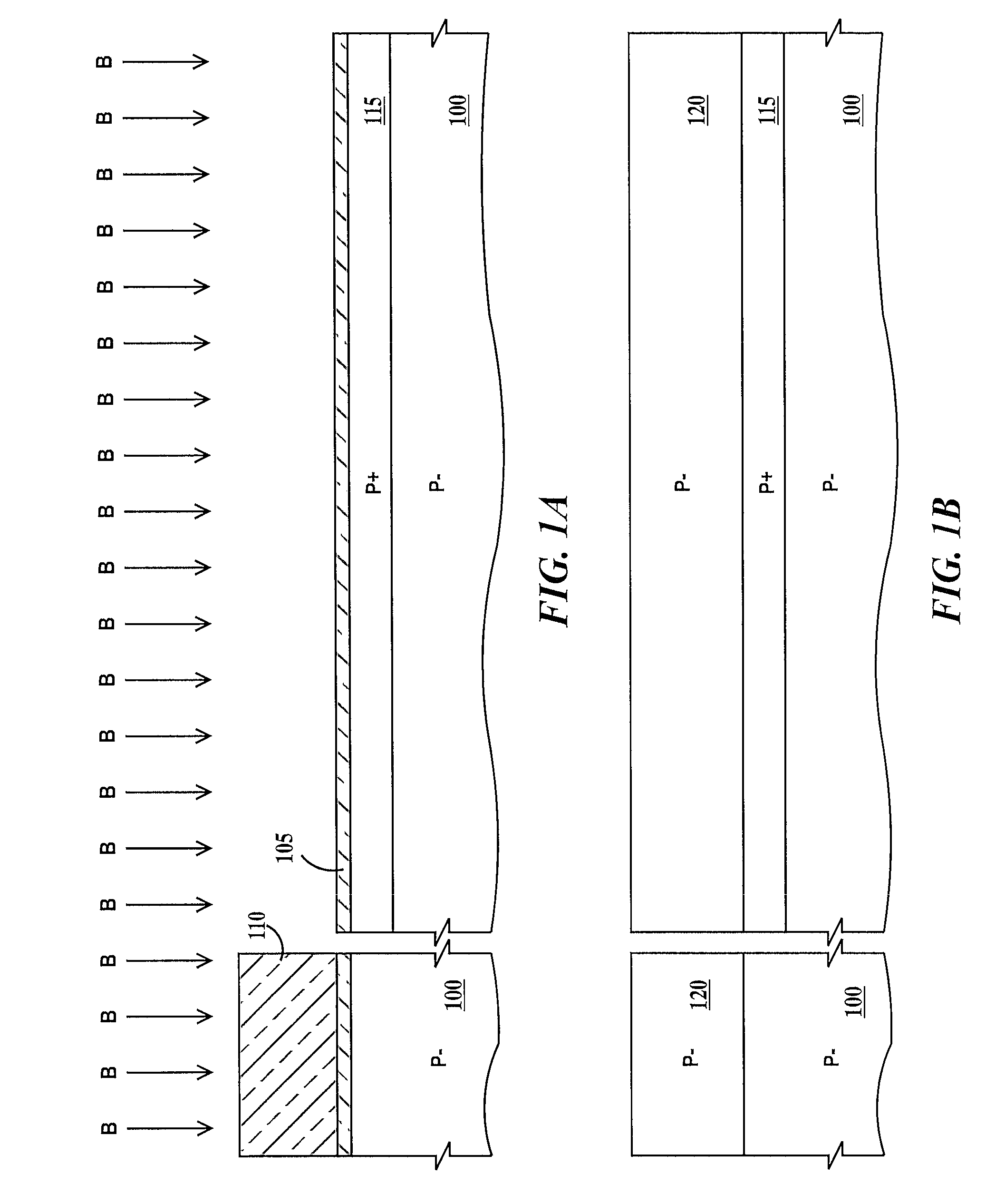
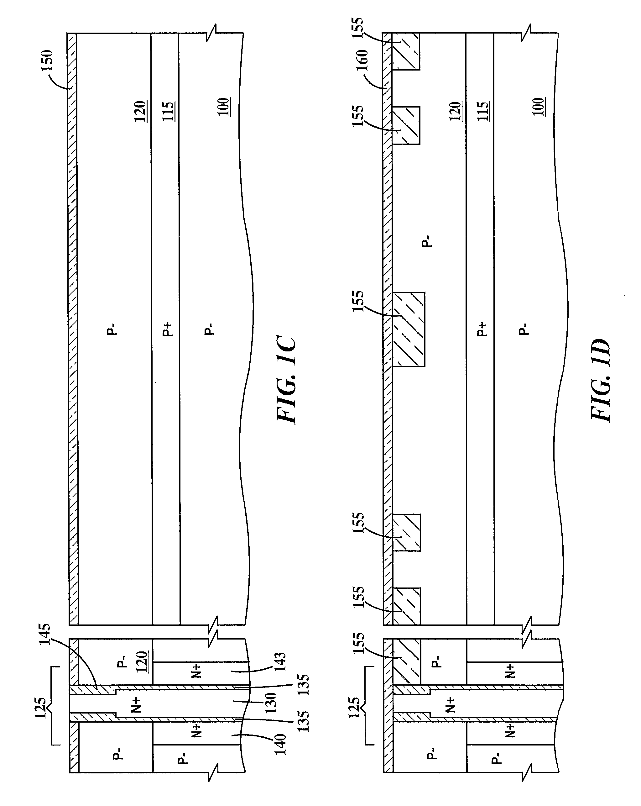
[0010]FIGS. 1A through 1I are cross-sectional views illustrating fabrication of CMOS devices according to embodiments of the present invention. In FIG. 1A, formed on a lightly doped P-type mono-crystalline silicon substrate 100 is a dielectric layer 105. In one example, substrate 100 is doped to a concentration between about 1E16 atm / cm3 and about 5E16 atm / cm3. In one example dielectric layer 105 is thermally grown silicon dioxide about 1 nm to about 10 nm thick. Formed on dielectric layer 105 is a patterned photoresist layer 110. In one example, patterned photoresist layer 110 may be formed by applying a layer of photoresist on dielectric layer 105, exposing the photoresist layer to actinic radiation through a patterned photomask, and developing the exposed photoresist layer to remove some regions of the exposed photoresist layer while leaving other regions of the exposed photoresist layer. Then a P-type ion-implantation is performed into substrate 100 to form highly P-doped region...


PUM


Abstract

A triple-well CMOS structure having reduced latch-up susceptibility and a method of fabricating the structure. The method includes forming a buried P-type doped layer having low resistance under the P-wells and N-wells in which CMOS transistors are formed and forming a gap in a buried N-type doped layer formed in the P-wells, the is gap aligned under a contact to the P-well. The buried P-type doped layer and gap in the buried N-type doped layer allow a low resistance hole current path around parasitic bipolar transistors of the CMOS transistors.

Description

RELATED APPLICATIONS [0001] This application is a division of co-pending U.S. patent application Ser. No. 11 / 340,344 filed on Jan. 26, 2006.FIELD OF THE INVENTION [0002] The present invention relates to the field of complimentary metal-oxide-silicon (CMOS) devices; more specifically, it relates to triple-well CMOS device structures and methods of fabricating triple-well CMOS device structures. BACKGROUND OF THE INVENTION [0003] Advanced embedded dynamic random access memories (EDRAMs) are fabricated with lightly P− type doped substrates using triple well structures in order to form buried diffused capacitor plates and to isolate the charge transfer NFET of the EDRAM. However, the combination of lightly P-type doped substrates and triple well structures includes parasitic NPN and PNP bipolar transistors in adjacent NFETs and PFETs which can form a parasitic latch and can go into latch-up mode (high current flow with feedback) when charge pairs are generated, for example, by heavy ion...

Claims


Application Information

Patent Timeline
Patent Type & Authority Applications(United States)
IPC IPC(8): H01L21/8238
CPCH01L27/0921H01L29/7833H01L29/1087H01L27/0928
Inventor CECCHI, DELBERT R.FURUKAWA, TOSHIHARUMANDELMAN, JACK ALLAN
Owner INT BUSINESS MASCH CORP
Why Eureka
Try Eureka