IGBT device with cavity bypass structure and manufacture method of IGBT device

A device and hole technology, applied in the field of semiconductor devices and their manufacturing, can solve the problems of IGBT device safety working area to be improved, IGBT device safety working area is small, and IGBT reliability is reduced, and the structure and design concept are compatible and improved. Effect of electric field distribution and improvement of reliability

Inactive Publication Date: 2016-10-19
STATE GRID CORP OF CHINA +2
View PDF4 Cites 0 Cited by
  • Summary
  • Abstract
  • Description
  • Claims
  • Application Information

AI Technical Summary

Problems solved by technology

[0005] The safe working area of ​​the existing IGBT device is small, which reduces the reliability of the IGBT. Therefore, the safe working area of ​​the existing IGBT device needs to be improved

Method used


Image

  • IGBT device with cavity bypass structure and manufacture method of IGBT device
  • IGBT device with cavity bypass structure and manufacture method of IGBT device
  • IGBT device with cavity bypass structure and manufacture method of IGBT device

Examples


Embodiment Construction

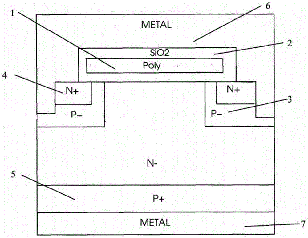
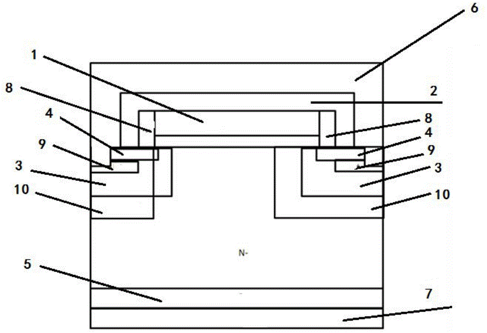
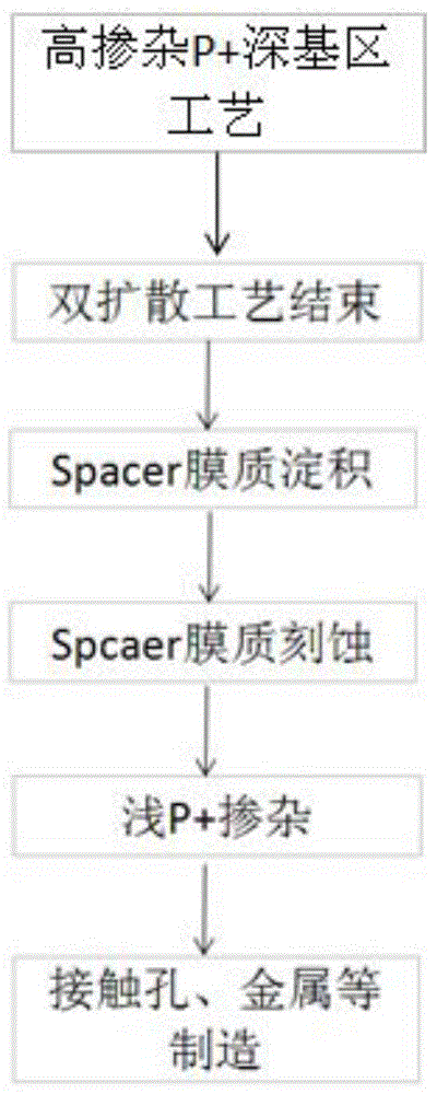
[0048] The specific implementation manners of the present invention will be further described in detail below in conjunction with the accompanying drawings.

[0049]The following description and drawings illustrate specific embodiments of the invention sufficiently to enable those skilled in the art to practice them. Other embodiments may incorporate structural, logical, electrical, process, and other changes. The examples merely represent possible variations. Individual components and functions are optional unless explicitly required, and the order of operations may vary. Portions and features of some embodiments may be included in or substituted for those of other embodiments. The scope of embodiments of the present invention includes the full scope of the claims, and all available equivalents of the claims. These embodiments of the present invention may be referred to herein, individually or collectively, by the term "invention", which is for convenience only and is not ...


PUM


Abstract

The invention relates to an IGBT device with a hole bypass structure and a manufacturing method thereof. A polycrystalline sidewall protection structure, a shallow P+ structure and a P+ deep base region are provided in the active region of the IGBT device; the polycrystalline sidewall protection The structure is located on both sides of the polysilicon gate; the shallow P+ structure is located between the N+ region and the P-base region; the P+ deep base region is set outside the P-base region and surrounds the P-base region to form a hole bypass structure. The invention introduces a highly doped P+ deep base region, improves hole flow distribution, improves electric field distribution, reduces parasitic thyristor latch, and improves IGBT reliability.

Description

technical field [0001] The invention relates to a semiconductor device and a manufacturing method thereof, in particular to an IGBT device with a hole bypass structure and a manufacturing method thereof. Background technique [0002] IGBT (Insulated Gate Bipolar Transistor) has the advantages of unipolar devices and bipolar devices at the same time, the driving circuit is simple, the control circuit power consumption and cost are low, the saturation voltage is low, and the device itself has small loss. It is the development of high voltage and high current in the future. direction. [0003] IGBT is a three-terminal device, including front emitter, gate and back collector. For the cross-sectional view of the active area of ​​the IGBT chip, see figure 1 , including the emitter 6 on the front, the gate 1 and the collector 7 on the back. The surface is a MOSFET structure, and the back is a parasitic PNP tube structure. Among them: 1 is the polysilicon gate, 2 is the gate oxi...

Claims


Application Information

Patent Timeline
Patent Type & Authority Applications(China)
IPC IPC(8): H01L29/739H01L21/335
Inventor 刘江赵哿高明超王耀华何延强吴迪曹功勋乔庆楠刘钺杨李晓平董少华李立金锐
Owner STATE GRID CORP OF CHINA
Why Eureka
Try Eureka