Integrated circuit capable of avoiding bolt-lock effect

A latch-up effect, integrated circuit technology, applied in circuits, electrical components, electro-solid devices, etc., can solve the problems of increasing circuit complexity and layout space, reduce the chance of latch-up effect, and improve the trigger level. Effect

Active Publication Date: 2007-07-04
WINBOND ELECTRONICS CORP
View PDF5 Cites 0 Cited by
  • Summary
  • Abstract
  • Description
  • Claims
  • Application Information

AI Technical Summary

Problems solved by technology

This method still increases circuit complexity and layout space

Method used


Image

  • Integrated circuit capable of avoiding bolt-lock effect
  • Integrated circuit capable of avoiding bolt-lock effect

Examples


Embodiment Construction

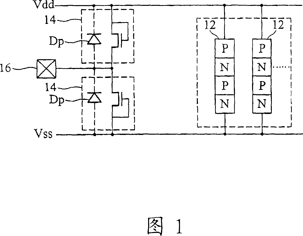
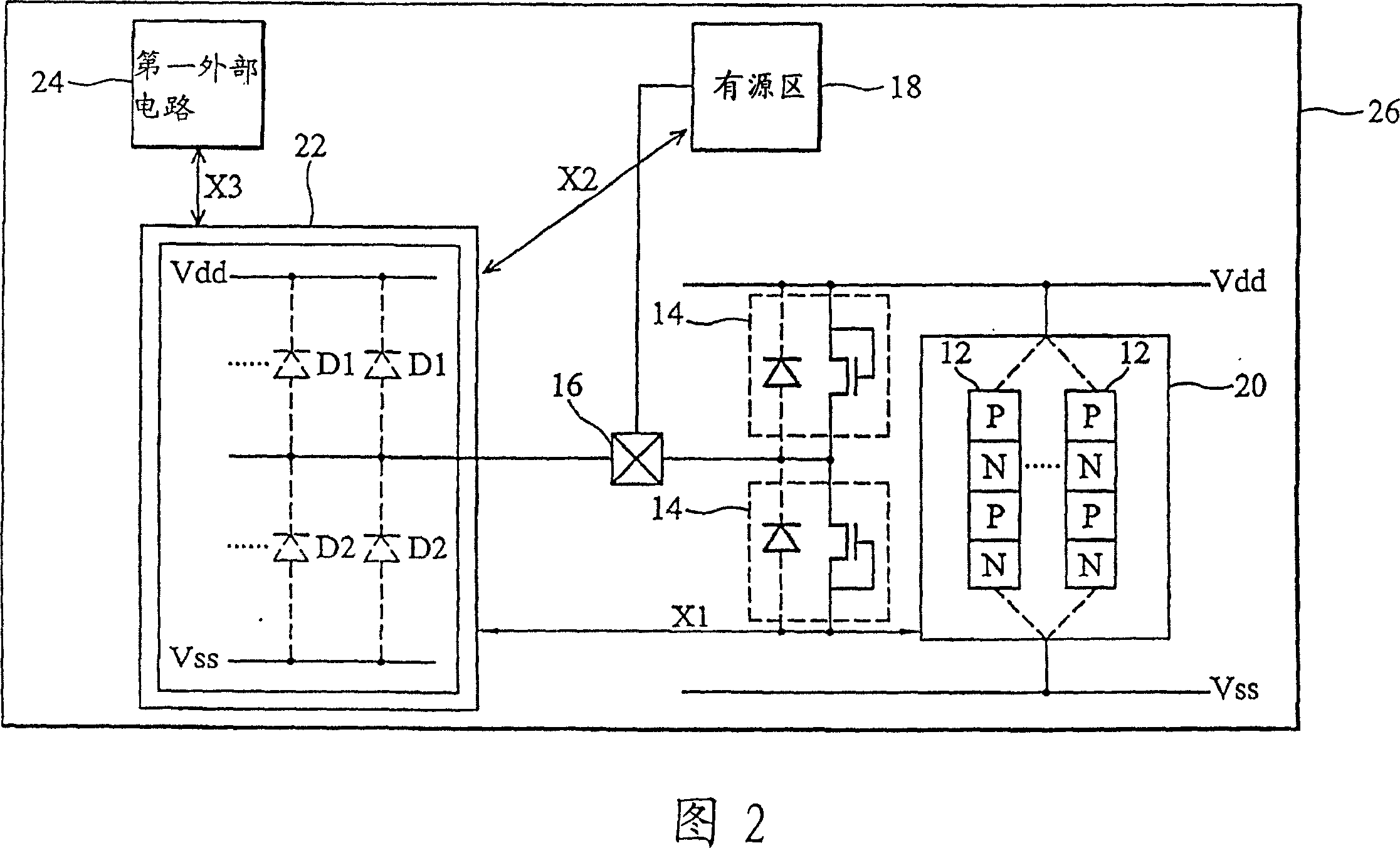
[0016] There are many factors that can cause latch-up in CMOS, however, the most obvious ones are substrate currents generated by hot carrier effects during IC operation, and / or caused by noise present on pads The forward current of the parasitic diode. And most of the substrate current generated by the latch-up effect is injected through the parasitic diode formed by the electrostatic discharge (ESD) protection circuit on the chip.

[0017] Unlike the prior art, the present invention uses a passive method of prohibiting conduction of the parasitic SCR to prevent the occurrence of latch-up effect. The spirit of the present invention is to reduce the influence of the trigger source of the latch-up effect by adding a shunt diode as the shunt path of the substrate current without changing the layout of the original internal circuit and ESD protection components, thereby reducing the chance of the latch-up effect occurring .

[0018] FIG. 2 is used to illustrate the method for a...


PUM


Abstract

An integrated circuit that can avoid bolt lock effect. It includes the internal circuit on the base plate with at least one SCR structure; at least one ESD protective groupware and a driving area on the base plate and are coupled a bonding sheet; at least the first shunt diode with a positive pole coupling the bonding sheet and a negative pole coupling a first voltage source; at least a second shunt diode with a negative pole coupling the bonding sheet and a positive pole coupling a second voltage source. The distance between the first and the second shunt diodes and the internal circuit, the distance between the ESD proactive groupware and the driving area is no less than 150 micron; a protective ring to surround the first and the second shunt diodes.

Description

technical field [0001] The invention relates to an integrated circuit, especially an integrated circuit which can avoid latch-up effect. Background technique [0002] Latchup is a very important reliability issue in CMOS ICs, and is a low impedance state formed by the conduction of a parasitic PNPN (Silicon Controlled Rectifier, SCR) structure. Since there is a low parallel impedance between the power line and ground when latch-up occurs, a large amount of power line current will exist between the power lines. If this current is not limited, this will cause logic errors, circuit malfunctions, or irreversible damage to the IC. Unfortunately, because P+ of PMOS, NWELL of NMOS, P substrate, N+ will form the structure of PNPN SCR, and this parasitic SCR structure will be generated in the CMOS process. [0003] There are many factors that can cause latch-up in CMOS, however, the most obvious are substrate currents generated by hot-carrier effects during IC operation, and / or by ...

Claims


Application Information

Patent Timeline
Patent Type & Authority Patents(China)
IPC IPC(8): H01L23/60H01L23/62H01L27/02H01L23/58H01L27/092H01L29/861
Inventor 林奕成
Owner WINBOND ELECTRONICS CORP
Why Eureka
Try Eureka