

Packaging Structure of Optical Devices
A technology of packaging structure and optical device, which is applied in the directions of optical device exploration, measurement device, electromagnetic wave re-radiation, etc., can solve the problems such as the overall volume reduction of the proximity optical sensor 100, reduce the chance of transmission to the photosensitive element, reduce the production Cost and manufacturing difficulty, the effect of reducing the overall volume and size
- Summary
- Abstract
- Description
- Claims
- Application Information
AI Technical Summary
Problems solved by technology
Method used
Image

Examples
Embodiment Construction
[0053] The aforementioned and other technical content, features and effects of the present invention will be clearly presented in the following detailed description of a preferred embodiment with reference to the drawings. The directional terms mentioned in the following embodiments, such as: up, down, left, right, front or back, etc., are only directions referring to the attached drawings. Accordingly, the directional terms are used to illustrate and not to limit the invention.
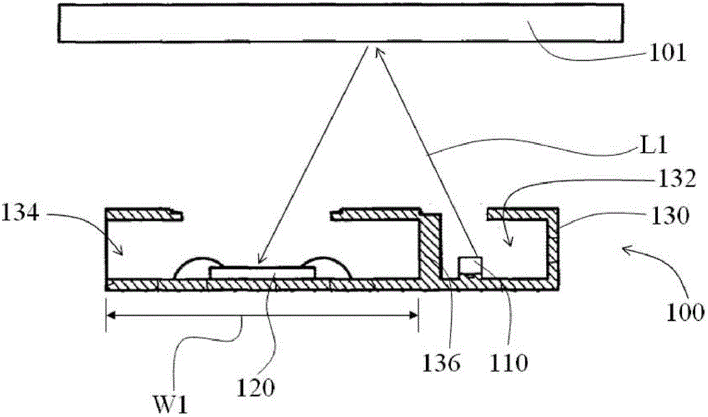
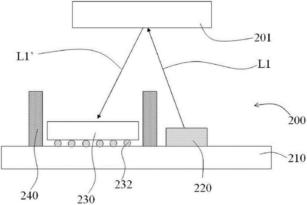
[0054] figure 2 It is a schematic diagram of a packaging structure of an optical device according to an embodiment of the present invention. The packaging structure 200 of the optical device in this embodiment can be illustrated by the structure of a proximity photosensor. Specifically, the packaging structure 200 of the optical device includes a substrate 210, a light emitting element 220, a photosensitive element 230, and a light blocking structure 240. . The light emitting element 220 is dispo...
PUM
 Abstract
Description
Claims
Application Information