Pen apparatus and method of assembly

a technology applied in the field of pen apparatus and assembly method, can solve the problems of delay negating polluted, z-axis related coordinate data, etc., and achieve the effects of high reliability, fabricability, and improved cost levels

Inactive Publication Date: 2007-08-23
SCRIPTEL CORP
View PDF14 Cites 35 Cited by
  • Summary
  • Abstract
  • Description
  • Claims
  • Application Information

AI Technical Summary

Benefits of technology

[0008] The present invention is addressed to pen apparatus for use with electrographic surfaces and a method of making it. Designed to incorporate a minimum number of parts which are assembled with minimized procedural steps, the apparatus enjoys a high level of reliability and is fabricable at improved cost levels.

Problems solved by technology

Such a delay negates polluted, z-axis related coordinate data.

Method used


Image

  • Pen apparatus and method of assembly
  • Pen apparatus and method of assembly
  • Pen apparatus and method of assembly

Examples


Embodiment Construction

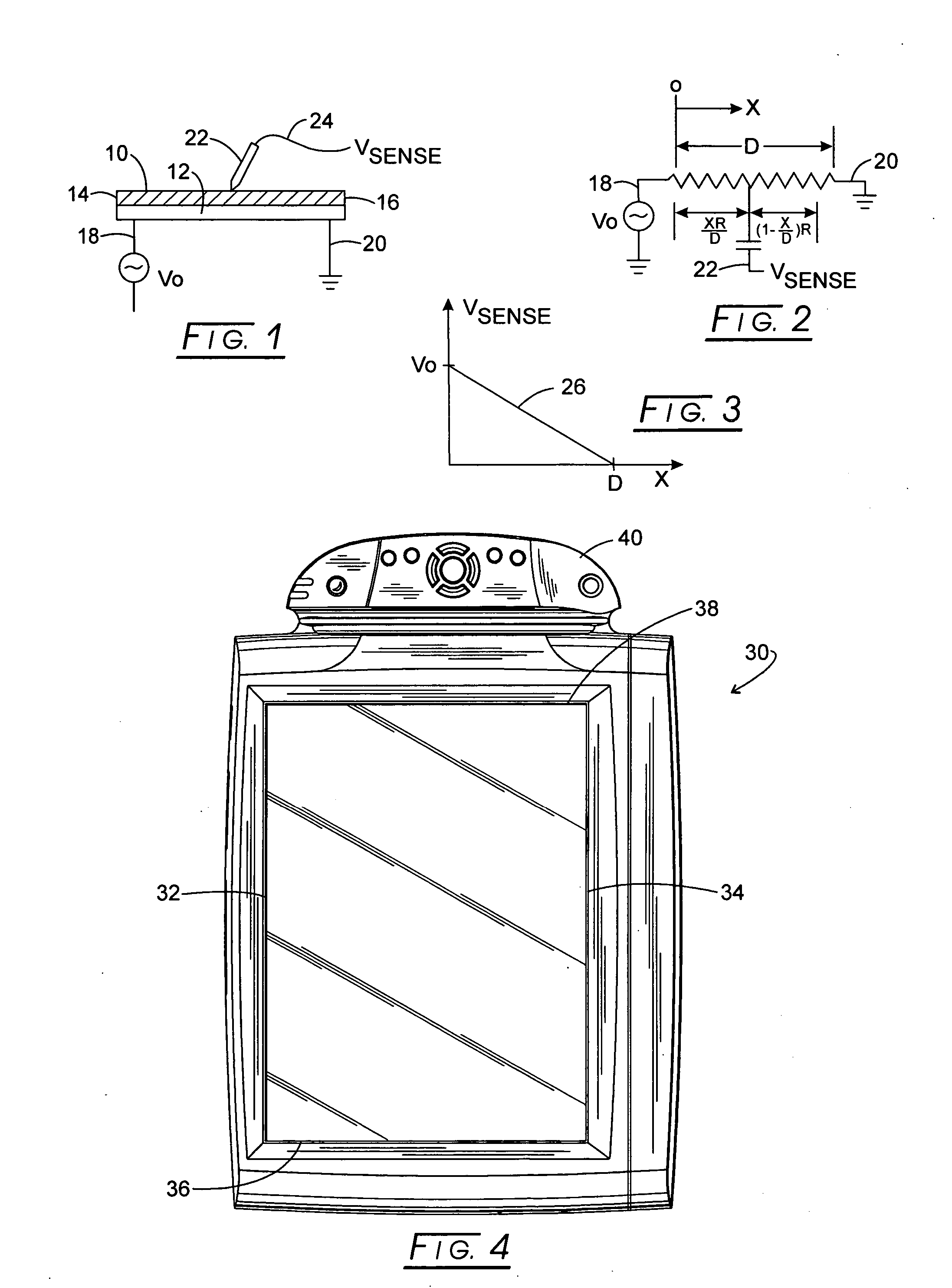
[0053] As a preliminary consideration of the general approach taken with resistant surface electrographic technology, reference is made to FIGS. 1 and 2 wherein an idealized one-dimensional model is revealed. In FIG. 1, an insulative support 10 such as glass is shown overlaying and supporting a resistive layer of, for example, indium-tin oxide 12. Electrodes 14 and 16 are shown coupled to the resistive layer 12 at the opposite ends or borders thereof. Electrode 14 is coupled with an a.c. source designated V0 from line 18, while electrode 16 is coupled to ground through line20. A pen 22 is positioned in contact with the glass support 10 which, through capacitive coupling serves to pick-up a voltage output at line 24, such voltage being labeled Vsense. The equivalent circuit for this idealized one-dimensional model is represented in FIG. 2 where the resistive layer 12 is shown as a resistor and the distance of the pen 22 from the edge of the resistor closest to the source V0 is repres...


PUM


Abstract

Pen apparatus and method of assembly wherein a pick-up rod assembly performs in conjunction with a normally closed switch to define a pen-up tip switch condition. Coordinate signal information is provided from the pick-up rod assembly to a signal treatment network carried by an elongate printed circuit board which supplies a bias and electrical communication to the pick-up rod assembly through an electrically conductive helical spring. That spring also provides switch closure bias and tip switch information is transferred from the switch to a pen orientation detector network at the circuit board through a stamped metal transition component. Bias generated at the signal treatment network is further utilized in providing tip switch information to the pen orientation detector network.

Description

CROSS-REFERENCE TO RELATED APPLICATIONS STATEMENT REGARDING FEDERALLY SPONSORED RESEARCH [0001] Not applicable. BACKGROUND OF THE INVENTION [0002] The history of technical development of electrographic devices is relatively short. At the present time, the operational quality of the now ubiquitous products is such that the terms “pen”, “paper” and “ink” are used in describing these computer driven interactive systems. Price and product reliability now have become significant factors in the electrographic market, the earlier significant challenges in technical development having been met. [0003] Early approaches to digitizer structures looked to an arrangement wherein a grid formed of two spaced arrays of mutually, orthogonally disposed fine wires was embedded in an insulative carrier. One surface of this structure served to yieldably receive a stylus input, which yielding caused the grid components to intersect and readout coordinate signals. Later approaches to achieving readouts we...

Claims


Application Information

Patent Timeline
Patent Type & Authority Applications(United States)
IPC IPC(8): G09G5/00B43K25/00G06F3/033
CPCG06F3/03545
Inventor KABLE, ROBERT G.KABLE, ADAM T.HERINGER, LAWRENCE J.WILSON, BRENT G.
Owner SCRIPTEL CORP
Why Eureka
Try Eureka