Pseudomorphic Si/SiGe/Si body device with embedded SiGe source/drain

a body device and sige technology, applied in the field of pseudomorphic si, can solve the problems of saturating the level of induced stress with these methods, affecting and generally disadvantageous performance of an nfet for the performance of p

Inactive Publication Date: 2007-08-23
IBM CORP
View PDF99 Cites 108 Cited by
  • Summary
  • Abstract
  • Description
  • Claims
  • Application Information

AI Technical Summary

Problems solved by technology

The stress components should be engineered and applied differently because the type of stress which is beneficial for the performance of an NFET is generally disadvantageous for the performance of the PFET.
While these methods do provide structures that have tensile stresses being applied to the NFET device

Method used


Image

  • Pseudomorphic Si/SiGe/Si body device with embedded SiGe source/drain
  • Pseudomorphic Si/SiGe/Si body device with embedded SiGe source/drain
  • Pseudomorphic Si/SiGe/Si body device with embedded SiGe source/drain

Examples


Embodiment Construction

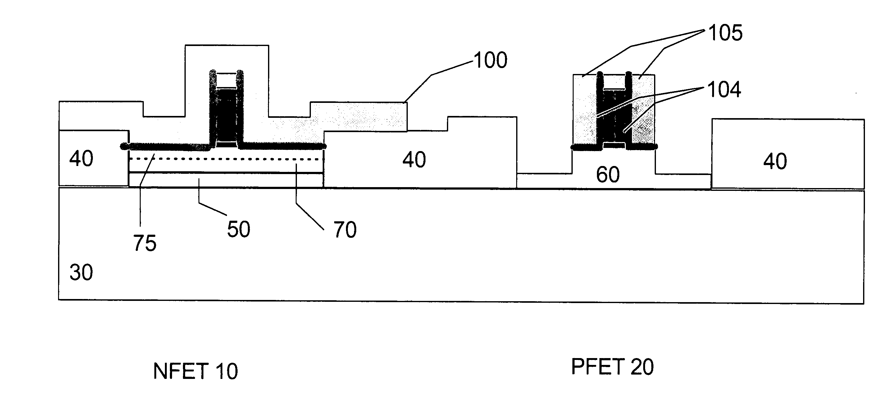
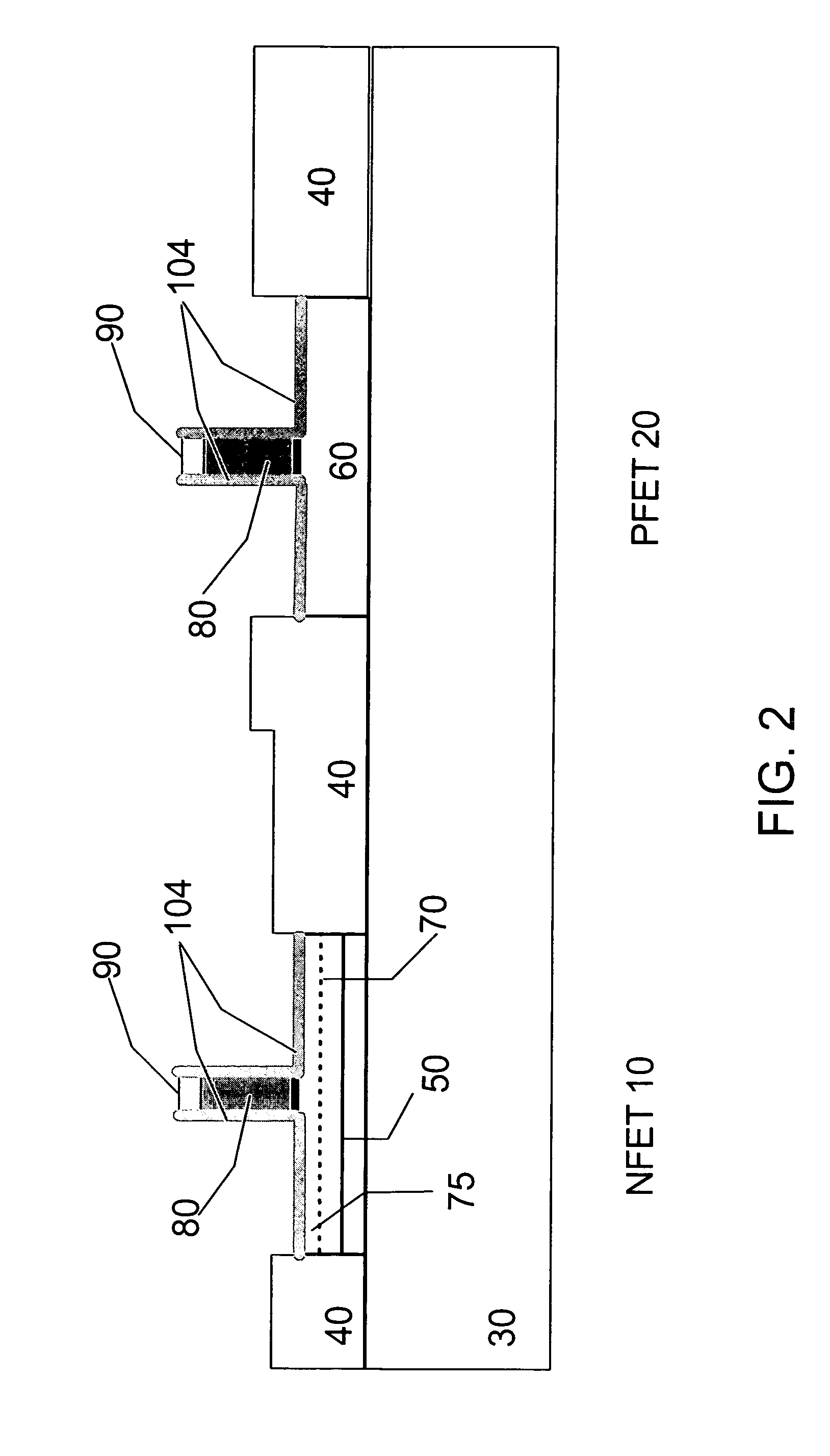
[0011] The invention relates to a semiconductor structure and method of manufacturing and more particularly to a CMOS device with at least one embedded SiGe layer in the source / drain region of the PFET, and at least one embedded SiGe layer in the channel region of the NFET. In one embodiment, the structure of the invention enhances the electron mobility in the NFET device, and further enhances the hole mobility in the PFET device. Additionally, by using the fabrication methods and hence achieving the final structure of the invention, it is possible to construct a compressively strained channel PFET and a tensile strained channel NFET on the same substrate, in same processing steps.

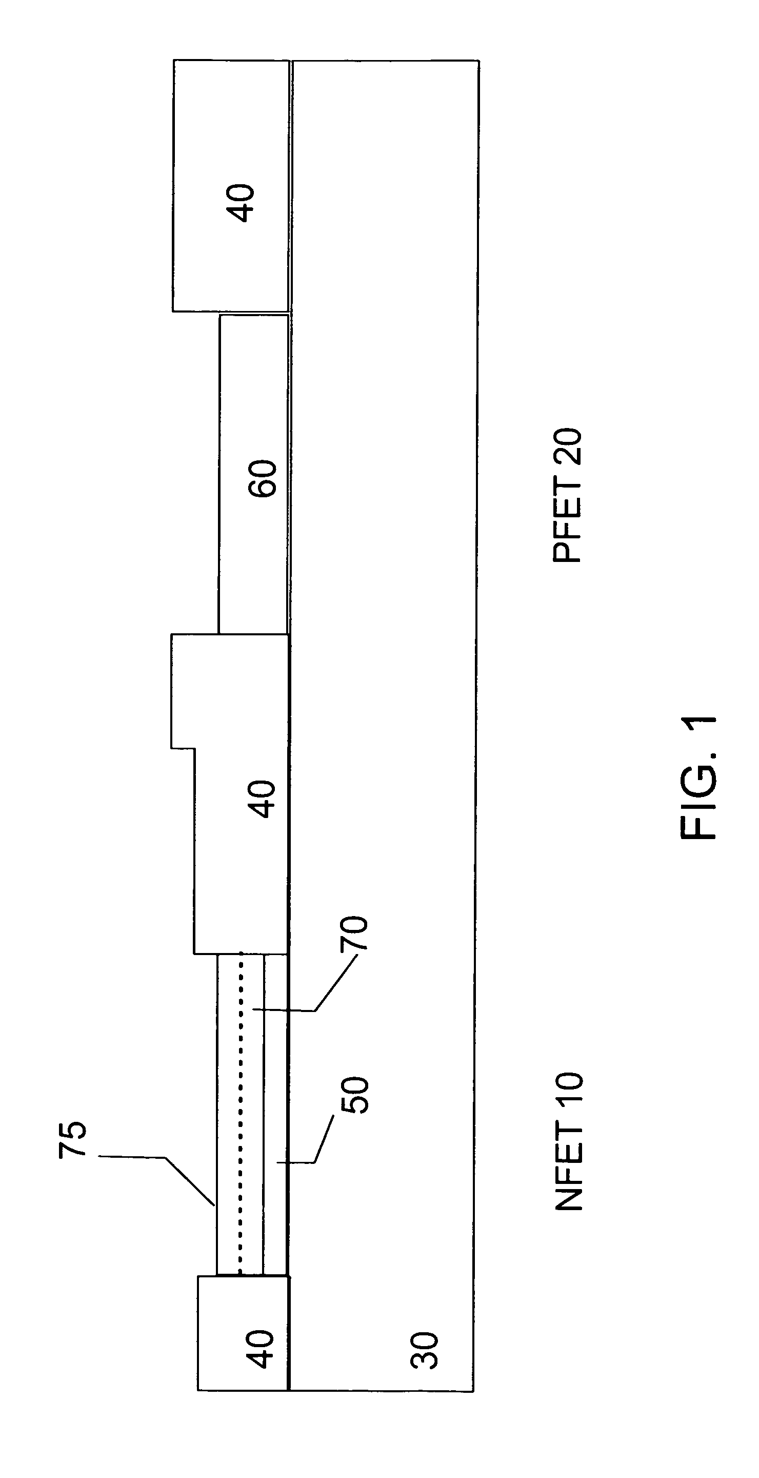
[0012] Referring to FIG. 1, an exemplary initial structure is shown. Specifically, the exemplary initial structure is comprised of an NFET region 10 and a PFET region 20 formed on a substrate 30. The substrate 30 can be any conventional substrate, for example, a buried oxide (BOX), or a conventional bulk ...


PUM


Abstract

The invention relates to a semiconductor structure and method of manufacturing and more particularly to a CMOS device with at least one embedded SiGe layer in the source/drain region of the PFET, and at least one embedded SiGe layer in the channel region of the NFET. In one embodiment, the structure of the invention enhances the electron mobility in the NFET device, and further enhances the hole mobility in the PFET device. Additionally, by using the fabrication methods and hence achieving the final structure of the invention, it is also possible to construct a PFET and NFET each with embedded SiGe layers on the same substrate.

Description

FIELD OF THE INVENTION [0001] The invention relates generally to a semiconductor device and method of manufacturing, and more particularly to a semiconductor device and method of manufacturing an NFET and PFET device with stress components. BACKGROUND DESCRIPTION [0002] Mechanical stresses within a semiconductor device substrate can modulate device performance. That is, stresses within a semiconductor device are known to enhance semiconductor device characteristics. Thus, to improve the characteristics of a semiconductor device, tensile and / or compressive stresses are created in the channel of the NFETs and / or PFETs. But, it is well known that stress components affect the behaviors NFET and PFET devices differently. [0003] In order to maximize the performance of both NFETs and PFETs within integrated circuit (IC) chips, the stress components should be engineered and applied differently for NFETs and PFETs. The stress components should be engineered and applied differently because th...

Claims


Application Information

Patent Timeline
IPC IPC(8): H01L21/336
CPCH01L21/823807H01L21/823814H01L21/823878H01L21/84H01L29/7848H01L29/165H01L29/665H01L29/66628H01L29/66636H01L27/1203
Inventor CHIDAMBARRAO, DURESETIMOCUTA, ANDA C.MOCUTA, DAN M.RADENS, CARL
Owner IBM CORP
Why Eureka
Try Eureka