Substrate with multilayer plated through hole and method for forming the multilayer plated through hole

Active Publication Date: 2007-08-30
ADVANCED SEMICON ENG INC
View PDF3 Cites 13 Cited by
  • Summary
  • Abstract
  • Description
  • Claims
  • Application Information

AI Technical Summary

Benefits of technology

[0008]It is an object of the present invention to provide a substrate with a multilayer plated through hole and a method for forming the multilayer plated through hole. The method for forming a multilayer plated through hole is to form a dielectric layer and a conductive layer on the inner surface of a through hole in a substrate by deposition. T

Problems solved by technology

However, the way to form a via hole by drilling cannot precisely control the thickness of the resulting dielectric layer.
This will cause the separation of the signal channel from the shielding layer to be non-uniform and even a short circuit.
The way of forming a via hole by drilling is inappropriate to a substrate with a multilayer plated through hole.
However, when at the period of division of the via hole or even application to an end-product, such separation of

Method used


Image

  • Substrate with multilayer plated through hole and method for forming the multilayer plated through hole
  • Substrate with multilayer plated through hole and method for forming the multilayer plated through hole
  • Substrate with multilayer plated through hole and method for forming the multilayer plated through hole

Examples


Embodiment Construction

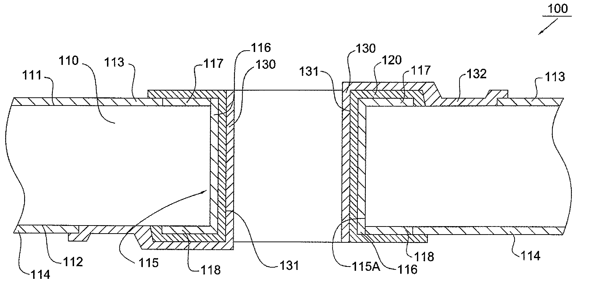
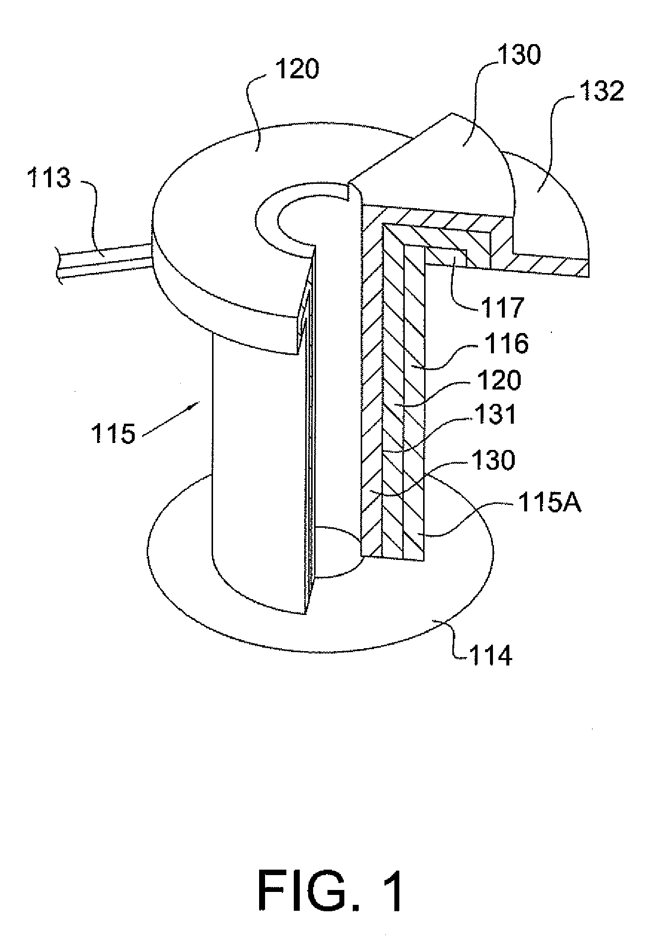
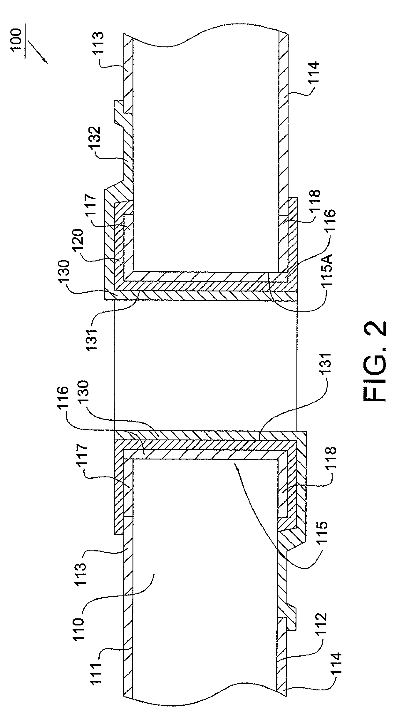
[0017]Referring to FIGS. 1 and 2, a substrate 100 with a multilayer plated through hole according to an embodiment of the present invention includes a substrate body 110 having opposing upper and lower surfaces 111, 112. The substrate body 110 can be a multilayer printed circuit board. The substrate body 110 has a first trace layer 113, a second trace layer 114 and a plated through hole 115. The first trace layer 113 is formed on the upper surface 111 of the substrate body 110 and the second trace layer 114 is formed on the lower surface 112 of the substrate body 110. The plated through hole 115 passes through the upper surface 111 to the lower surface 112. The plated through hole 115 includes an electroless plating layer 115A and a first conductive layer 116 that the two layers 115A and 116 electrically connect the first trace layer 113 to the second trace layer 114. In this embodiment, the first trace layer 113 includes a first terminal 117 and the second trace layer 114 includes ...


PUM


Abstract

A structure with a multilayer plated through hole is disclosed. At least one dielectric layer formed by deposition and a conductive layer are formed in an original plated through hole (PTH). The dielectric layer partially covers wiring layers of the substrate to electrically isolate the PTH and the conductive layer to form a multilayer PTH so as to save PTH occupation space of the substrate. Preferably, the formation of the dielectric layer is electrophoretic deposition to control the deposition thickness in the PTH very even and thin, no drilling is necessary. Accordingly, it can increase electrical performance and decrease cross-talk effect.

Description

CROSS REFERENCE TO RELATED APPLICATION [0001]This application claims the priority benefit of Taiwan Patent Application Serial Number 095106584 filed Feb. 27, 2006, the full disclosure of which is incorporated herein by reference.BACKGROUND OF THE INVENTION [0002]1. Field of the Invention[0003]The present invention relates to a multilayer circuit board and the method for manufacturing the same, and more particularly, to a substrate with a multilayer plated through hole and the method for forming the multilayer plated through hole.[0004]2. Description of the Related Art[0005]In general, multilayer circuit boards are frequently used in most electronic devices as media for signal transmission, power supply and grounding. As the electronic devices get complex and have more function, the number of trace layers of the multilayer circuit boards and longitudinal electrical connections between the trace layers are becoming greater. Accordingly, it is required to form much more plated through ...

Claims


Application Information

Patent Timeline
IPC IPC(8): H05K1/11H01R12/04
CPCH05K1/0222H05K1/115H05K2203/135H05K2201/09809H05K3/428
Inventor WANG, CHIEN HAO
Owner ADVANCED SEMICON ENG INC
Why Eureka
Try Eureka