

Dual operational mode CML latch
- Summary
- Abstract
- Description
- Claims
- Application Information
AI Technical Summary
Benefits of technology
Problems solved by technology
Method used
Image

Examples
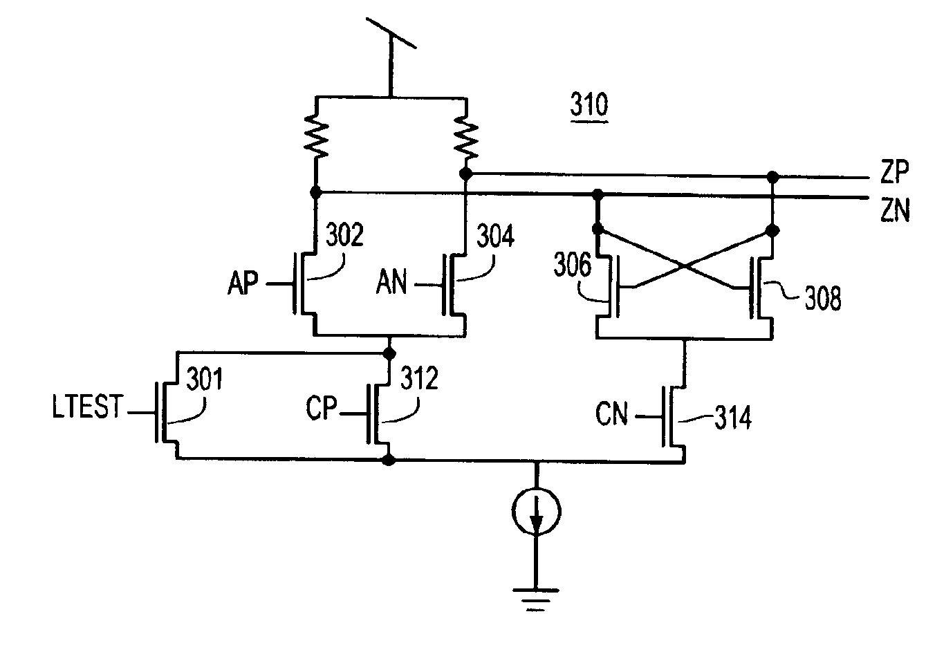
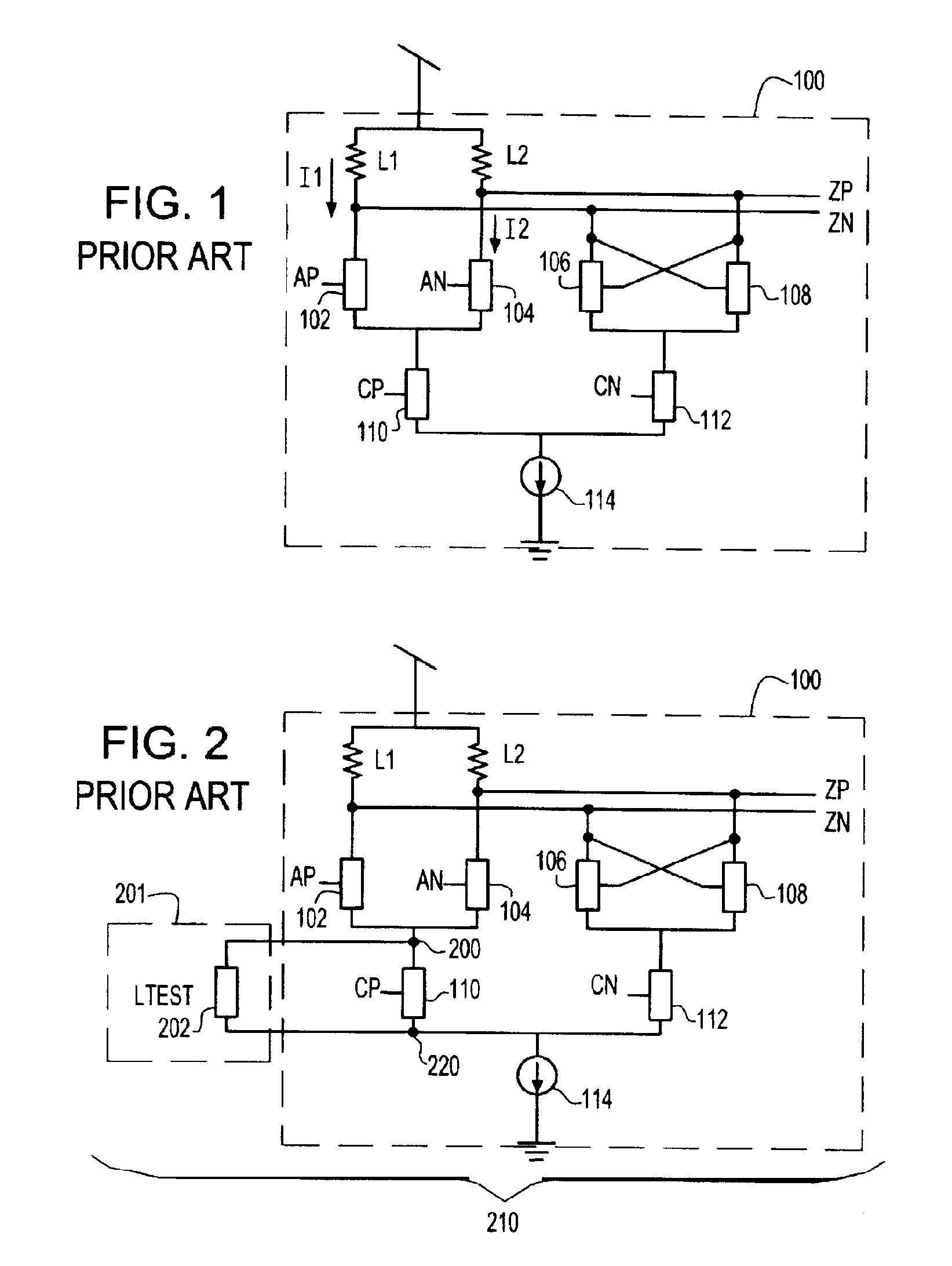
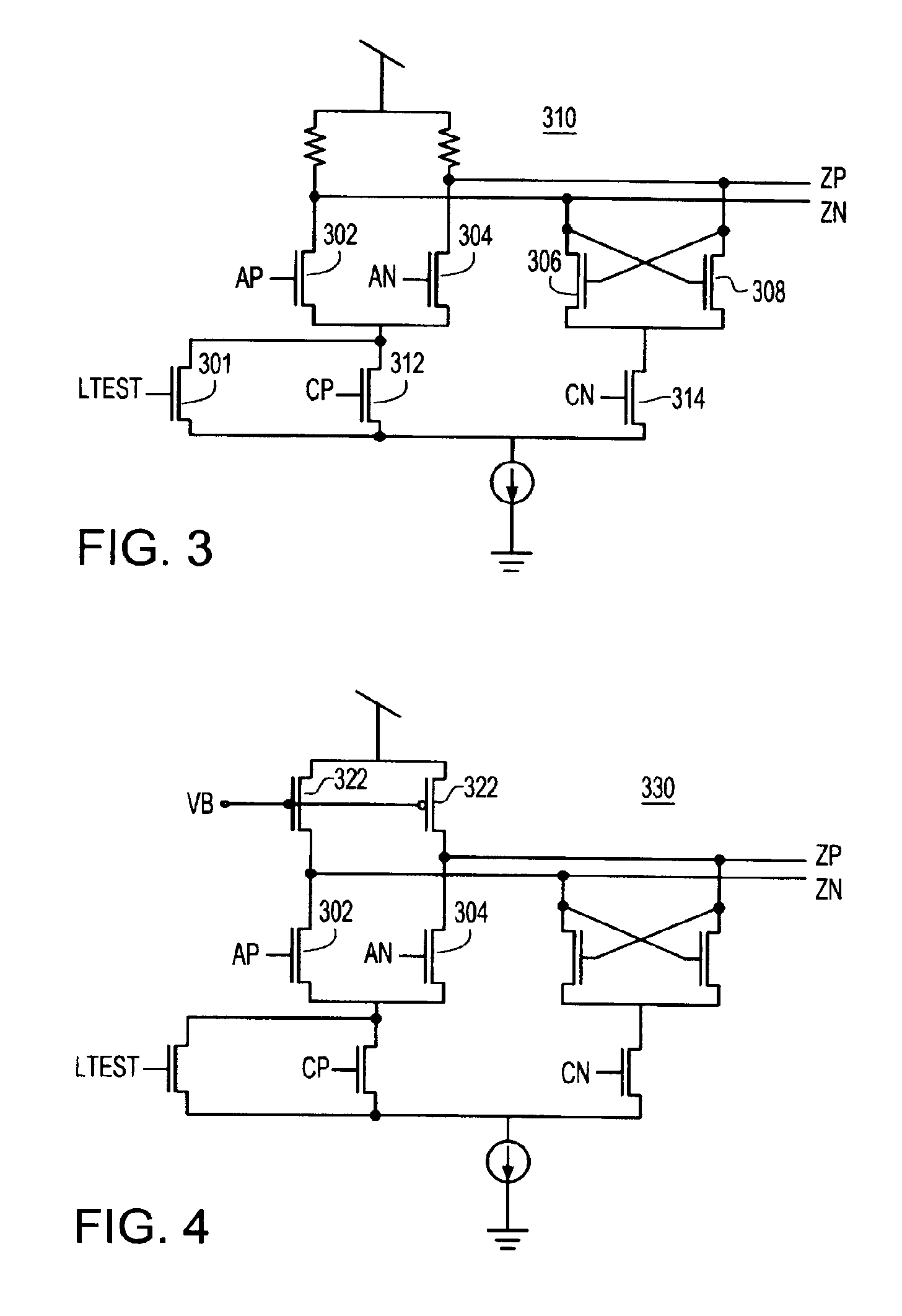
embodiment 310
[0030]FIG. 6A illustrates a CML latch 610 circuit according to yet another variation in which each of the mode control device 601, input devices 602, 604 and cross-coupled devices 606, 608 and tail devices 612, 614 of a are implemented as npn-type bipolar transistors. Operation is the same or similar to that described above with respect to the NFET embodiment 310 illustrated in FIG. 3. In a CML latch circuit 620 (FIG. 6B) according to a variation of the embodiment shown in FIG. 6A, pnp type active load devices 625, 627 or other appropriate active load devices are utilized in place of the load resistors R1 and R2.
embodiment 510
[0031]FIG. 6C illustrates a CML latch circuit 630 according to a further variation in which each of the mode control device 631, input devices 632, 634 and cross-coupled devices 646, 648 and tail devices 642, 644 are implemented as pnp-type bipolar transistors. Operation is similar if not functionally nearly the same as that described above with respect to the PFET embodiment 510 illustrated in FIG. 5A. In a CML latch circuit according to a further variation 650 (FIG. 6D), npn type active load devices 535, 537 or other appropriate active load devices are utilized in place of the load resistors R1 and R2.
[0032]FIG. 7 is a block and schematic diagram illustrating a serializer circuit 700 in accordance with a further embodiment of the invention. The serializer circuit incorporates CML latch circuits in accordance with any one or more of the embodiments described above with respect to FIGS. 2 through 6D. Specifically, each of the flip-flops and latches in the serializer circuit 700 incl...
PUM
 Abstract
Description
Claims
Application Information