Electro-optical device, light receiving device, and electronic apparatus

a technology of optical devices and electronic devices, applied in the direction of optics, semiconductor devices, instruments, etc., can solve the problems of increasing the number of processes, increasing the number of man-hours and costs, and inability to obtain sufficient light sensitivity, etc., to achieve the effect of optimizing the display

Inactive Publication Date: 2007-08-30
JAPAN DISPLAY WEST
View PDF11 Cites 18 Cited by
  • Summary
  • Abstract
  • Description
  • Claims
  • Application Information

AI Technical Summary

Benefits of technology

[0031]With such a configuration, outside light can be detected at high sensitivity, which makes it possible to optimize displaying in accordance with illuminance of outer light, and the like.

Problems solved by technology

Accordingly, the optical sensor needs to be implemented on a flexible print substrate, causing increased number of man-hour and cost.
When the mask conductive layer is remaining on the intrinsic layer, introduction of light to the intrinsic layer is restricted by the mask conductive layer, so that sufficient light sensitivity can not be obtained.
Consequently, in the PIN type diode formed region, it is required to provide a process for removing the mask conductive layer, so that there is a problem in that the number of processes is increased.
On the other hand, during light receiving, the light introduced from the light receiving side surface is difficult to be introduced into the intrinsic layer.

Method used


Image

  • Electro-optical device, light receiving device, and electronic apparatus
  • Electro-optical device, light receiving device, and electronic apparatus
  • Electro-optical device, light receiving device, and electronic apparatus

Examples


first embodiment

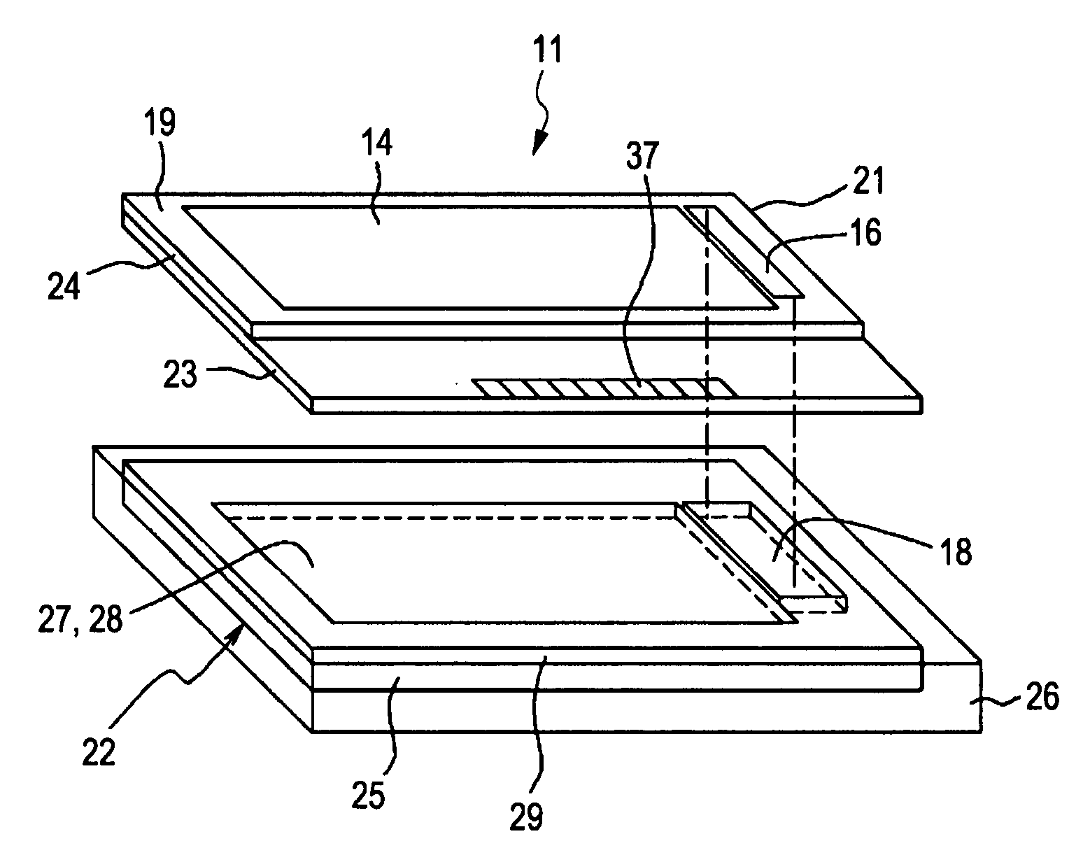
[0043]In FIGS. 1 and 2, the electro-optical device 11 is constructed by a display panel 21 constructed by sticking two substrates together. When a liquid crystal panel is employed as the display panel 21, as shown in FIG. 1, the electro-optical device 11 includes a display panel 21 and a lighting unit 22. Note that a display panel of a self emission type may also be employed as for the electro-optical device. In this case, there is no need for the lighting unit 22.

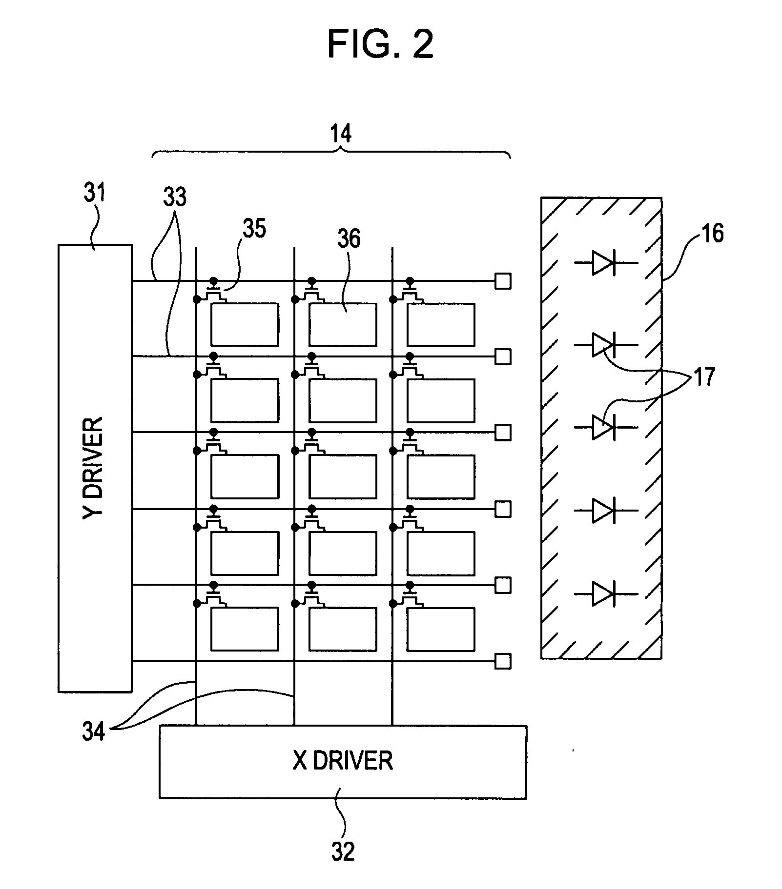
[0044]Liquid crystal (not shown) is enclosed between an element substrate 23 and an opposing substrate 24 through which light is transmitted to construct the display panel 21. The oppositely disposed element substrate 23 and opposing substrate 24 are bonded with a seal member (not shown). The display panel 21 includes, for example, a plurality of scanning lines 33 (see FIG. 2) provided so as to extend in the lateral direction and a plurality of data lines 34 (not shown) provided so as to extend in the vertical direction in...

second embodiment

[0083]FIG. 6 is a perspective view schematically showing an electro-optical device according to a second embodiment of the invention. In FIG. 6, like reference numerals are used to denote like elements in FIG. 1 and their descriptions will be omitted.

[0084]In the embodiment, only position and shape of the light receiving element disposed region and position and shape of the reflecting portion opposing the light receiving element disposed region are different from that of the first embodiment.

[0085]The electro-optical device 111 is constructed by a display panel 121 and a lighting unit 122 having the same structure as the first embodiment. An element substrate 123, an opposing substrate 124, a light shielding region 119, and a light receiving element disposed region 116 each corresponds to the element substrate 23, the opposing substrate 24, the light shielding region 19, and the light receiving element disposed region 16 of the first embodiment. The light receiving element disposed ...

third embodiment

[0089]FIG. 7 is a cross sectional view schematically showing an electro-optical device according to a third embodiment of the invention. In FIG. 7, like reference numerals are used to denote like elements in FIG. 3 and their descriptions will be omitted.

[0090]In the first embodiment, the surface of the reflecting plate is, for example, flat. In this case, the reflecting direction of the light introduced to the reflecting plate is determined by an incidence angle. Accordingly, there is a possibility that most of the introduced light is not introduced into the light receiving diode.

[0091]Accordingly, in the embodiment, by providing concavities and convexities on the surface of the reflecting plate, most of outside light is to be introduced into the light receiving diode. In the embodiment, the lighting unit 132 is different from the lighting unit 22 of the first embodiment at the point in which the reflecting portion 133 is employed instead of the reflecting portion 18.

[0092]The refle...


PUM

PropertyMeasurementUnit
widthaaaaaaaaaa
lengthaaaaaaaaaa
widthaaaaaaaaaa

Abstract

An electro-optical device includes a transparent substrate, a PIN type diode formed in the transparent substrate and receiving light introduced through a light receiving side surface of the transparent substrate, and a reflecting portion provided on a surface side opposite to the light receiving side surface of the transparent substrate and for reflecting light passed through the transparent substrate to the PIN type diode.

Description

BACKGROUND[0001]1. Technical Field[0002]The present invention relates to an electro-optical device, a light receiving device, and an electronic apparatus which are preferable for a display equipment or the like for performing control of display luminance.[0003]2. Related Art[0004]A liquid crystal panel is constructed by enclosing liquid crystal between two substrates such as a glass substrate, a quartz substrate or the like. An electrode is provided on each substrate and an image signal is supplied to the electrodes. Optical property of liquid crystal positioned between electrodes of each substrate changes in accordance with the image signal. That is, alignment of liquid crystal molecules is changed by applying a voltage to the liquid crystal positioned between electrodes of each substrate based on the image signal. Thereby transmittance of light in each pixel is changed in accordance with the image signal and image display in accordance with the image signal is performed.[0005]In o...

Claims


Application Information

Patent Timeline
Patent Type & Authority Applications(United States)
IPC IPC(8): G02F1/1335
CPCG02F1/13318G02F1/133553H01L31/153G02F2001/133612H01L27/14G02F1/1362G02F1/133612
Inventor KOIDE, SHINMURAMATSU, HIROKOFUJITA, SHIN
Owner JAPAN DISPLAY WEST
Why Eureka
Try Eureka