Semiconductor device

Inactive Publication Date: 2007-09-13
LAPIS SEMICON CO LTD
View PDF6 Cites 5 Cited by
  • Summary
  • Abstract
  • Description
  • Claims
  • Application Information

AI Technical Summary

Benefits of technology

[0022]According to the invention, the surface area of the lower surface of the substrate on which the semiconductor chip from which a substantial amount of heat is generated, is increased. As a r

Problems solved by technology

In the conventional semiconductor devices of such structures, it is becoming more difficult to ensure radiation of heat from the lower surface of the substrate on which a semiconductor chip is mou

Method used


Image

  • Semiconductor device
  • Semiconductor device
  • Semiconductor device

Examples


embodiment 1

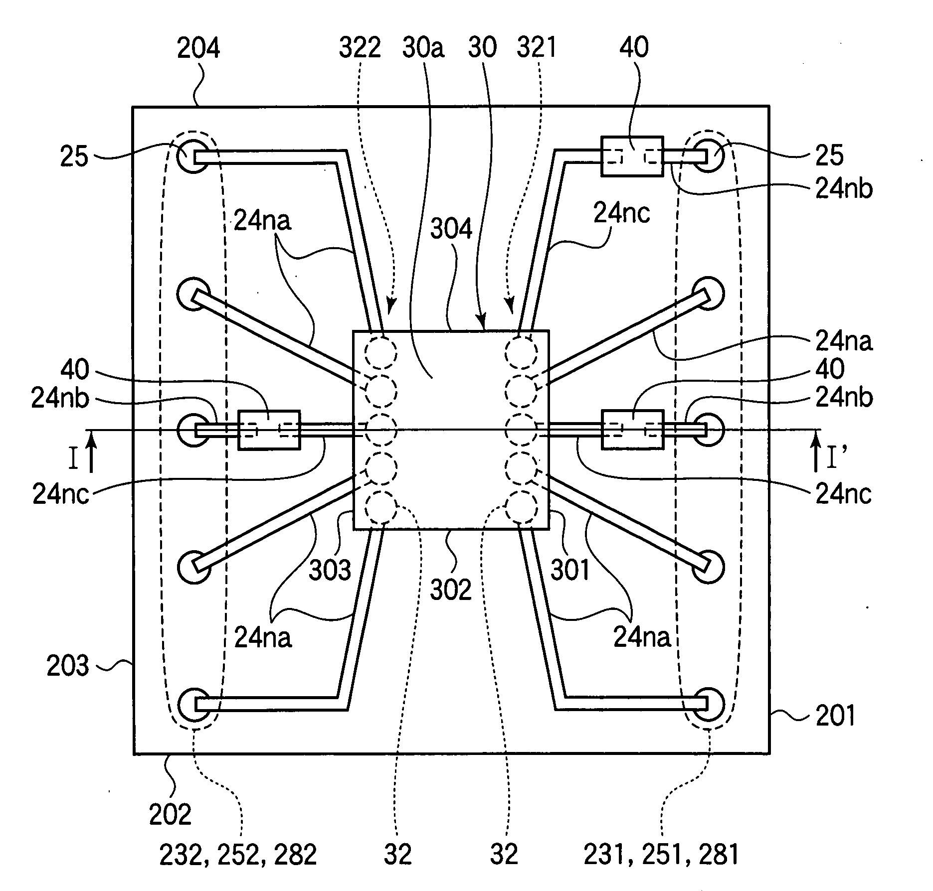
[0030]A semiconductor device of Embodiment 1 of the present invention will now be described referring to FIG. 1A, FIG. 1B and FIG. 2.

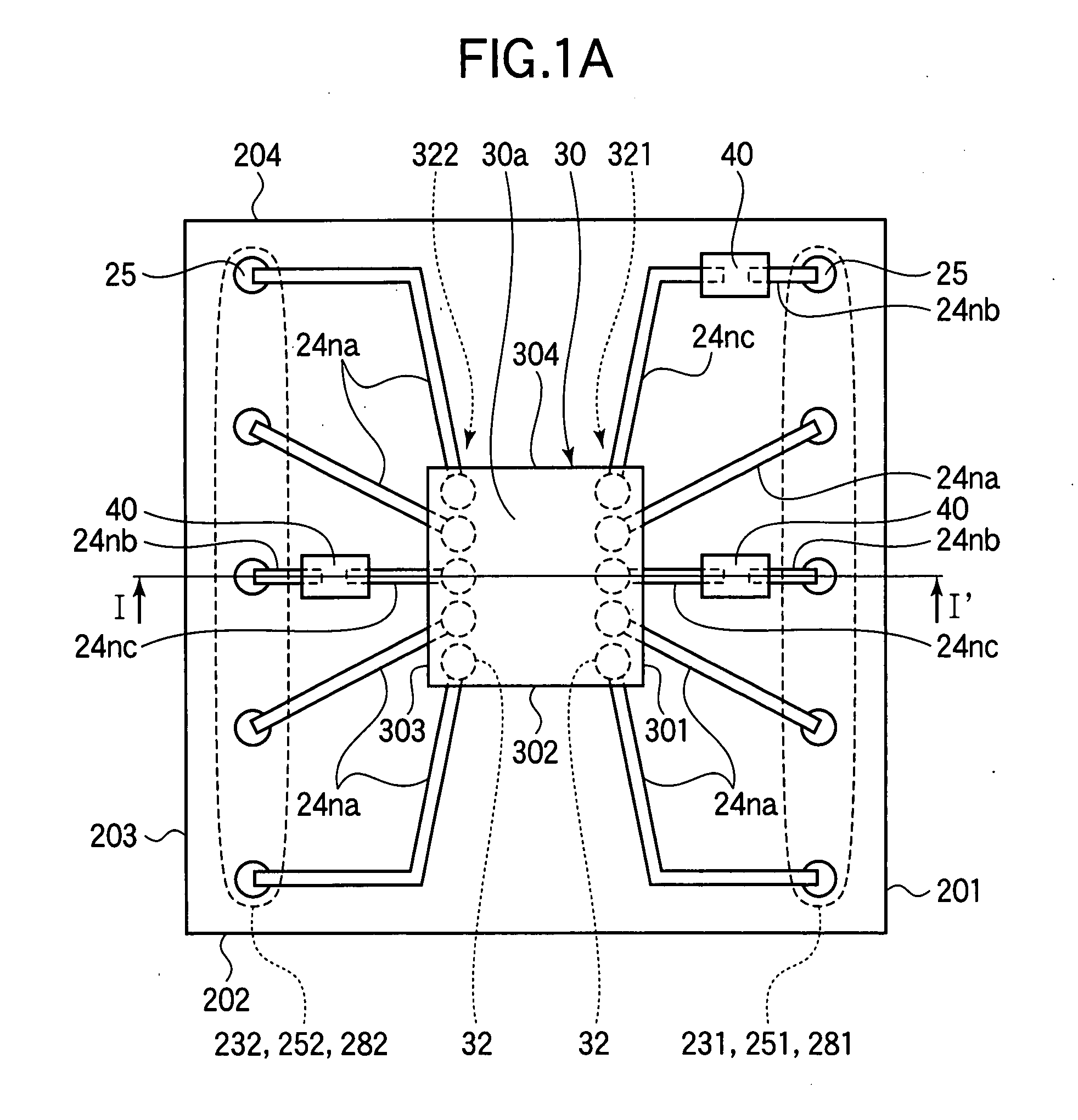
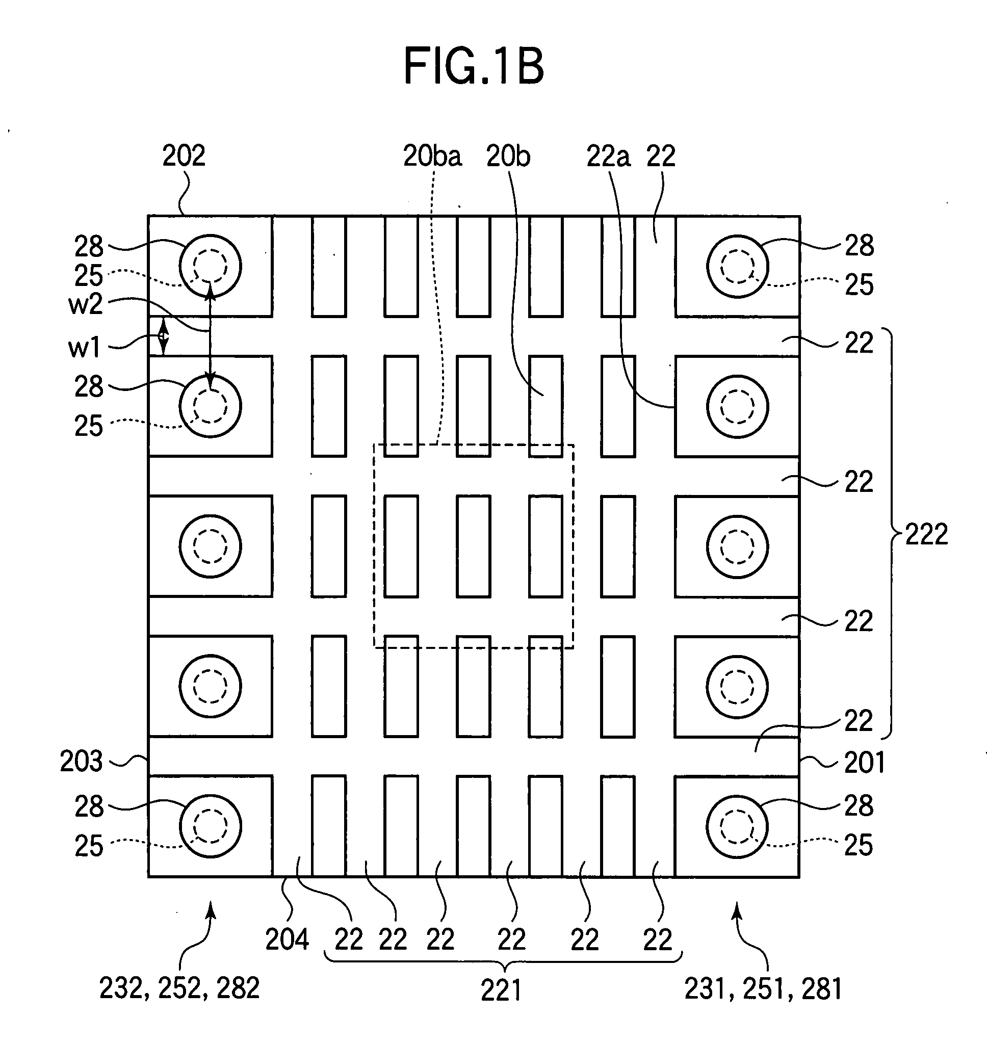
[0031]FIG. 1A is a plan view of a semiconductor device of Embodiment 1, and FIG. 1B is a bottom view of the semiconductor device of Embodiment 1. FIG. 2 is a schematic sectional view along line I-I′ in FIG. 1A.

[0032]As shown in FIG. 2, the semiconductor device (module) 10 includes a substrate 20. The substrate 20 is preferably a silicon substrate, for example. However, the substrate 20 may be a substrate of metal such as aluminum, a glass substrate, an organic resin substrate such as a glass epoxy substrate, a flexible print substrate, or the like.

[0033]The substrate 20 has a first main surface (upper surface) 20a, and a second main surface (lower surface) 20b opposite to the first main surface 20a. In the illustrated example, the first main surface 20a and the second main surface 20b are both rectangular, and more specifically square, in shape. The su...

embodiment 2

[0070]A semiconductor device of Embodiment 2 of the invention will next be described with reference to FIG. 3.

[0071]FIG. 3A is a bottom view of the semiconductor device of Embodiment 2. FIG. 3B is a schematic cross sectional view along the line II-II′ in FIG. 3A. The plan view of the semiconductor device of Embodiment 2 will be the same as FIG. 1A.

[0072]The semiconductor device of Embodiment 2 is similar to the semiconductor device of Embodiment 1, but is additionally provided with a heat radiating member 50 provided on the second main surface 20b of the substrate 20. That is, the semiconductor device 10 of Embodiment 2 is identical to the semiconductor device 10 of Embodiment 1, except for the addition of the heat radiating member 50. Accordingly, parts or members identical to those in Embodiment 1 are identified by the same reference numerals, and their description is omitted.

[0073]The substrate 20 has a first main surface 20a, and a second main surface 20b opposite to the first m...


PUM


Abstract

A semiconductor device 10 includes a silicon substrate 20 having a first interconnection layer 24, a second interconnection layer 26, and grooves 22 provided at the second main surface 20b. Mounted on the substrate 20 are one or more semiconductor chips 30 having chip external terminals 32 electrically connected to the first interconnection layer; and one or more peripheral chips 40 electrically connected to the fist interconnection layer on the silicon substrate. By the provision of the grooves 22, the heart radiating property is improved.

Description

BACKGROUND OF THE INVENTION[0001]The present invention relates a semiconductor device, in particular to a semiconductor device with improved heat radiating property.[0002]Due to the development of the process technology of semiconductor devices in recent years, the process rule and the size of the semiconductor device are becoming smaller and smaller. Moreover, the demands on the semiconductor device for more increased integration and more increased output power are becoming more and more stronger.[0003]It is thus increasing more desired to improve the radiation of heat from semiconductor chips contained in the semiconductor device, in order to prevent failure in operation, and damages to the semiconductor device due to the heat generated by the semiconductor chip, and the poor heat radiation of the semiconductor device packages.[0004]To meet with the demands, and to prevent the bending of a substrate due to the heat generated by the semiconductor chips, Japanese Patent Kokai Public...

Claims


Application Information

Patent Timeline
IPC IPC(8): H01L29/76
CPCH01L23/367H01L2224/16225H01L25/0655H01L2924/15159H01L2924/15311H01L2924/19105
Inventor SHIRAISHI, YASUSHI
Owner LAPIS SEMICON CO LTD
Why Eureka
Try Eureka