Method of compensating for write power of a light source in an optical disk apparatus and optical disk apparatus using the method

Inactive Publication Date: 2007-09-13
SAMSUNG ELECTRONICS CO LTD
View PDF6 Cites 9 Cited by
  • Summary
  • Abstract
  • Description
  • Claims
  • Application Information

AI Technical Summary

Benefits of technology

[0017] It is therefore a feature of an embodiment of the present invention to provide a method of compensating for a write power of a light source in an optical disk apparatus to increase write quality by optimizing the write power in a write operation and an optical disk apparatus using the same.

Problems solved by technology

Furthermore, in view of the development of new optical disks, it is impossible to set optimum write parameters for all optical disks available on the market.
Moreover, even for common optical disks, previously stored write parameters may not be optimal, e.g., due to differences between optical disk apparatuses, individual differences between the optical disks, and/or operational environments.
However, even if the optimum write power is selected using the OPC, a write characteristic may be degraded due to an error of the optimum write power generated due to one or more of the following reasons.
First, there may be a difference between surface write characteristics at different locations of an optical disk.
This difference may be generated because the write power of a light source, which is optimum when the OPC is performed, may not be the optimum write power in a user data area.
In other words, since the surface write character

Method used


Image

  • Method of compensating for write power of a light source in an optical disk apparatus and optical disk apparatus using the method
  • Method of compensating for write power of a light source in an optical disk apparatus and optical disk apparatus using the method
  • Method of compensating for write power of a light source in an optical disk apparatus and optical disk apparatus using the method

Examples


Example

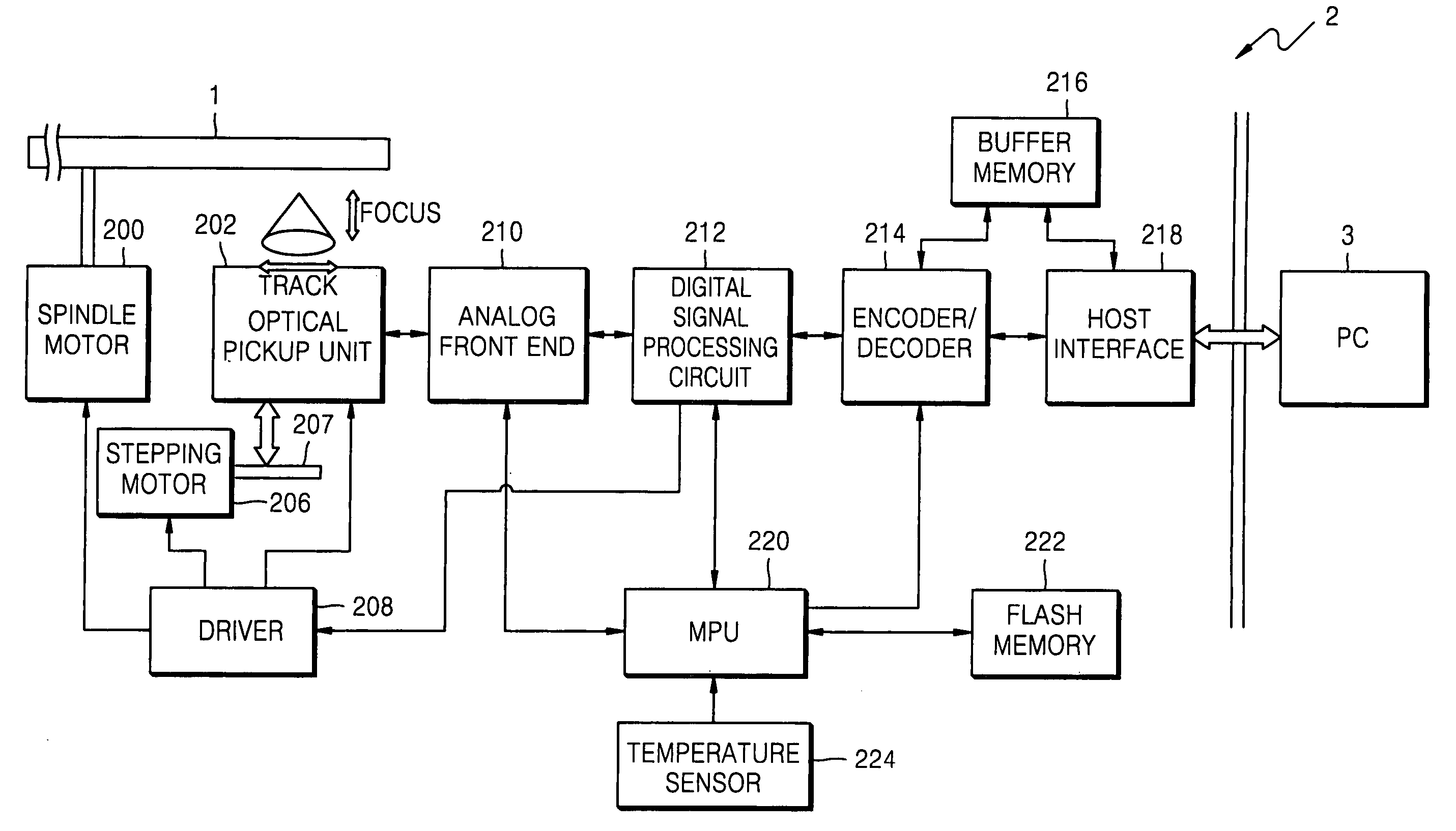
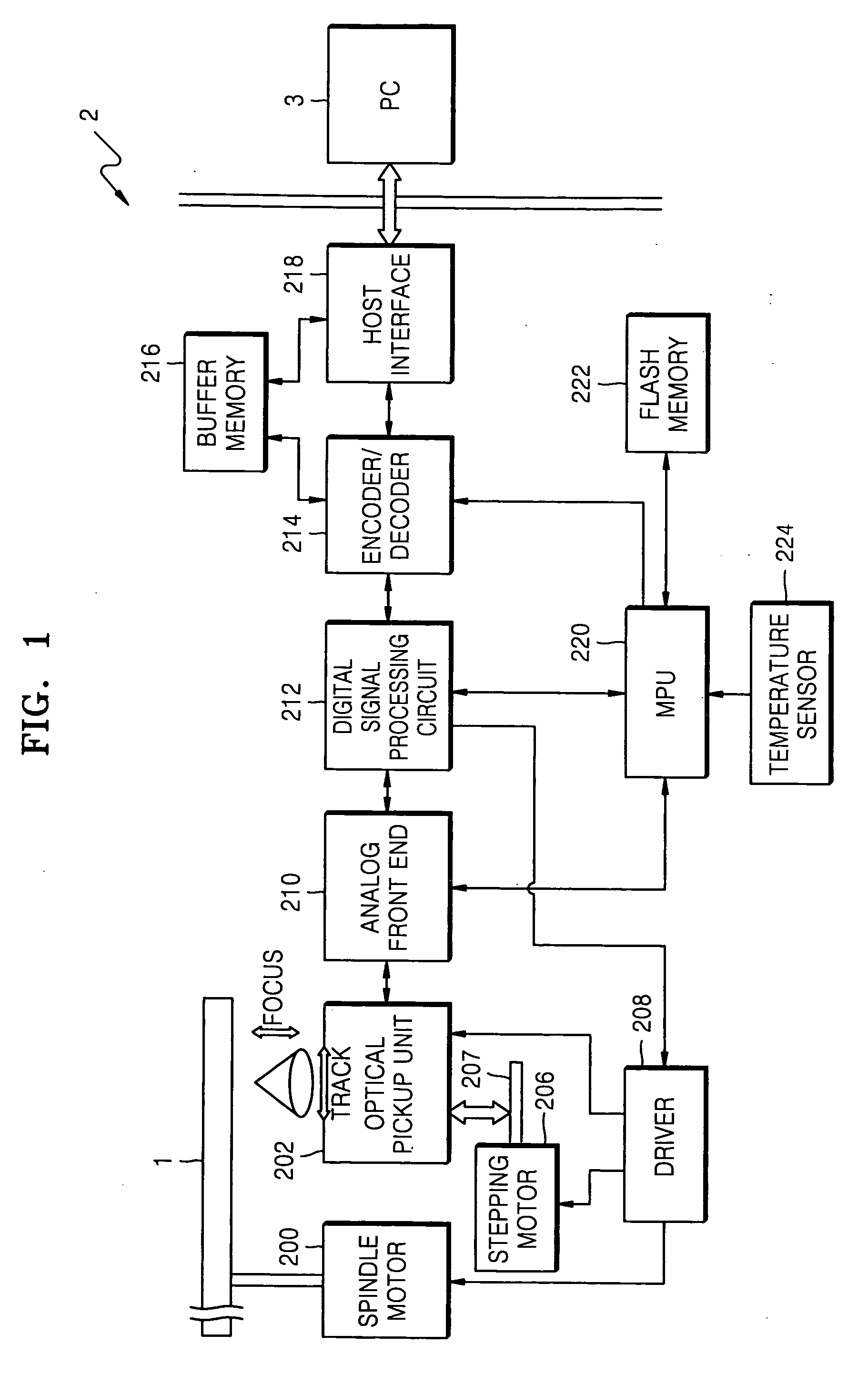
[0041] Japanese Patent Application No. 2005-372962, filed on Dec. 26, 2005, in the Japanese Patent Office, and entitled: “Method of Compensating for Write Power of Laser Beam in Optical Disk Apparatus and Optical Disk Apparatus Using the Method,” is incorporated by reference herein in its entirety.

[0042] The present invention will now be described more fully hereinafter with reference to the accompanying drawings, in which exemplary embodiments of the invention are illustrated. The invention may, however, be embodied in different forms and should not be construed as limited to the embodiments set forth herein. Rather, these embodiments are provided so that this disclosure will be thorough and complete, and will fully convey the scope of the invention to those skilled in the art. Like reference numerals refer to like elements throughout.

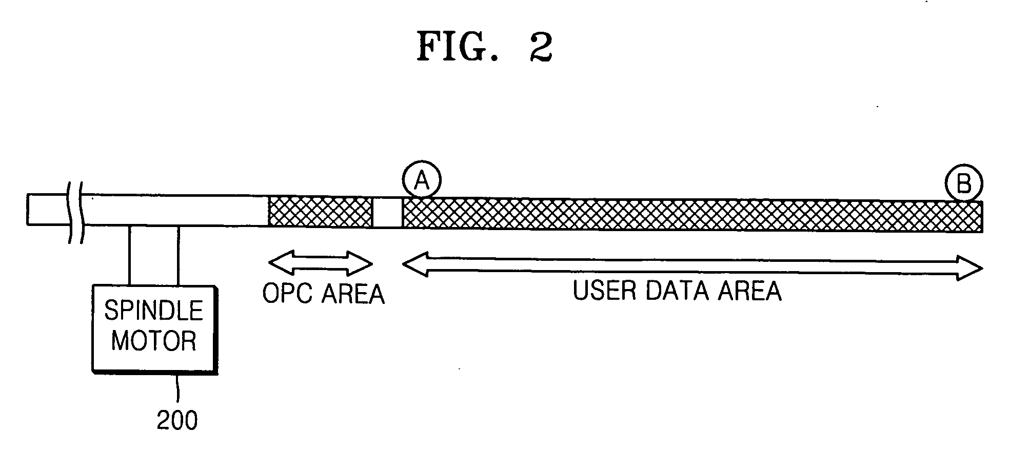
[0043] As will be described in detail below, according to embodiments of the present invention, write power may be compensated for by stopping a wr...


PUM


Abstract

A method of compensating for a write power of a laser beam in an optical disk apparatus may include determining whether a predetermined write condition is satisfied, stopping a write operation if the predetermined write condition is not satisfied, measuring a write characteristic of a recording area right before stopping the write operation, and compensating for the write power for recording the information based on the measured write characteristic. The optimum write power of a light source may be compensated for when a current write length exceeds a predetermined write length from a write start location, when a current temperature in a driver is outside a predetermined temperature range, and/or when a reflected light intensity from an optical disk in a write operation is outside a predetermined light intensity range.

Description

BACKGROUND OF THE INVENTION [0001] 1. Field of the Invention [0002] The present invention relates to a method of recording information on an optical disk. More particularly, the present invention relates to a method of compensating for write power of a light source while recording information and an optical disk apparatus performing the method. [0003] 2. Description of the Related Art [0004] Optical disks may generally be used as recording media for storing digital information, e.g., data, audio and video. Optical disks may be classified into postscript type optical disks, e.g., compact disc-read only (CD-R), rewrite type optical disks such as CD-RW (read and write), and bulk optical disks, e.g., digital versatile disc (DVD)-R, DVD±R, DVD±RW, and DVD±RAM (random access memory). Current trends include miniaturizing a spot diameter using a high numerical aperture (NA) object lens, using increasingly shorter wavelength light sources, e.g., a semiconductor laser, and using a thin printe...

Claims


Application Information

Patent Timeline
IPC IPC(8): G11B7/125
CPCG11B7/1267G11B7/1263G11B7/0045
Inventor TOMISHIMA, YUICHIRO
Owner SAMSUNG ELECTRONICS CO LTD
Why Eureka
Try Eureka