Driving circuit structure of liquid crystal panel

Inactive Publication Date: 2014-03-27
TCL CHINA STAR OPTOELECTRONICS TECH CO LTD
View PDF3 Cites 5 Cited by
  • Summary
  • Abstract
  • Description
  • Claims
  • Application Information

AI Technical Summary

Benefits of technology

[0032]In one embodiment of the present invention, trace widths of the trace portions of the COFs are gradually increased, and intensity of the output signals of the gate driving COFs are identical.
[0033]In the present invention, by gradually increasing the trace widths of the trace portions of the gate driving COFs along the gate

Problems solved by technology

However, in actual operation, the liquid crystal panel 90 will generate one problem: the liquid crystal panel 90 will ap

Method used


Image

  • Driving circuit structure of liquid crystal panel
  • Driving circuit structure of liquid crystal panel
  • Driving circuit structure of liquid crystal panel

Examples


Example

[0038]The foregoing objects, features and advantages adopted by the present invention can be best understood by referring to the following detailed description of the preferred embodiments and the accompanying drawings. Furthermore, the directional terms described in the present invention, such as upper, lower, front, rear, left, right, inner, outer, side and etc., are only directions referring to the accompanying drawings, so that the used directional terms are used to describe and understand the present invention, but the present invention is not limited thereto.

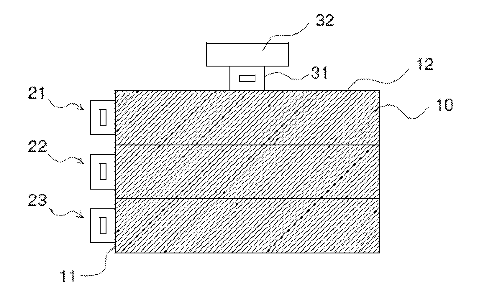
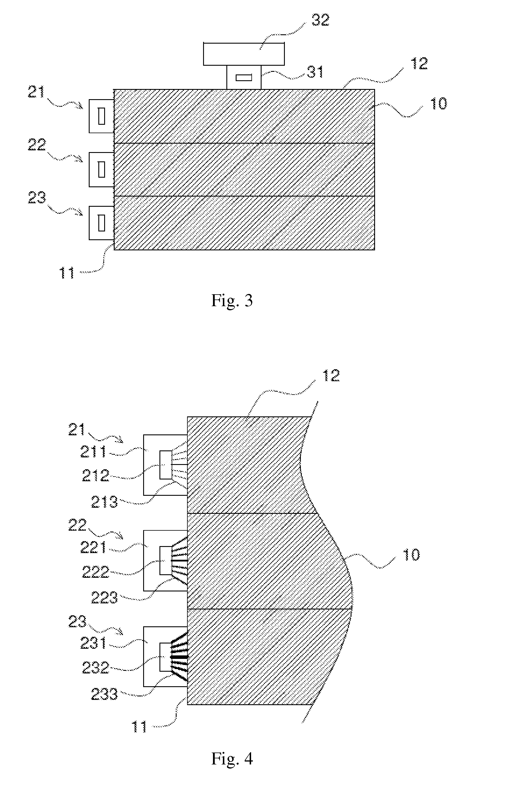
[0039]Referring now to FIGS. 3 and 4, a top view of a driving circuit structure of a liquid crystal panel according to the present invention is illustrated in FIG. 3; and a partially enlarged view of FIG. 3 is illustrated in FIG. 4. Specially explaining, for conveniently describing, FIGS. 3 and 4 are shown in simplification, wherein the number of the traces is simplified, and some of details which are unrelated to the expl...


PUM


Abstract

The present invention discloses a driving circuit structure of a liquid crystal panel, which mainly comprises a liquid crystal panel. The liquid crystal panel has an edge of a gate driving circuit and an edge of a source driving circuit. The edge of the gate driving circuit is provided with a plurality of gate driving COFs (chip on film). In the present invention, by gradually increasing trace widths of trace portions of the gate driving COFs along a gate scanning direction, the intensity of output signals of the gate driving COFs can be identical. Hence, it can eliminate the phenomenon of apparent boundary line that is appeared between the gate driving COFs of the liquid crystal panel, so as to increase the display quality.

Description

FIELD OF THE INVENTION[0001]The present invention relates to a driving circuit structure of a liquid crystal panel, and more particularly to a driving circuit structure of a liquid crystal panel which has gradually increasing trace widths of trace portions of gate driving COFs (chip on film) along a gate scanning direction.BACKGROUND OF THE INVENTION[0002]A liquid crystal display (LCD) is a type of flat panel display (FPD) which displays images by the property of the liquid crystal material. In comparison with other display devices, the LCD has the advantages in lightweight, compactness, low driving voltage and low power consumption, and thus has already become the mainstream product in the whole consumer market. In a traditional process of LCD panel, it comprises a front-end array process, a mid-end cell process and a back-end modulation process. The front-end array process is used to produce thin-film transistor (TFT) substrates (also called array substrates) and color filter (CF)...

Claims


Application Information

Patent Timeline
IPC IPC(8): G09G3/36
CPCG09G3/36G02F1/13452
Inventor DONG, CHENGCAIHSU, JEHAO
Owner TCL CHINA STAR OPTOELECTRONICS TECH CO LTD
Why Eureka
Try Eureka