
Quasi-vertical LDMOS device having closed cell layout

a closed cell, quasi-vertical technology, applied in the direction of semi-conductor devices, basic electric elements, electrical equipment, etc., can solve the problems of limiting the current handling capability of the device, challenging and often times more expensive design of the mosfet, and inability to meet the needs of power management applications, etc., to achieve the effect of low-voltage power devices

Active Publication Date: 2007-09-20
CICLON SEMICON DEVICE
View PDF84 Cites 30 Cited by
  • Summary
  • Abstract
  • Description
  • Claims
  • Application Information

AI Technical Summary

Benefits of technology

[0008] A low voltage power device is provided. The power device includes a plurality of quasi-vertical MOS device cells arranged in a closed cell configuration. In embodiments, the closed cell configuration is a checkerboard or hexagonal arrangement.

Problems solved by technology

When used in PWM applications, the transistors must exhibit small power loss during switching, which imposes an additional requirement—small internal capacitances—that make the MOSFET design challenging and often times more expensive.
The thick epitaxial layer and P+ substrate results in a high on resistance (Rds,on) in the device, which is not acceptable for power management applications as explained above.
This in turn leads to a de-biasing effect known for lateral devices (voltage drop along a stripe electrode under high current conditions) and limits the current handling capability of the device.
The reported reliability problems are due to the bipolar action of the parasitic NPN transistor formed by the source, body and drift regions.
This approach, however, is limited by the design rule requesting that a specific distance between the P+ contact and the polysilicon gate be kept larger than a minimum value defined by the technology generation, i.e., 0.5 μm for a 0.5 μm technology.
As yet, the technologies described above have not met the demand for an improved specific Rds,on and size for low voltage power devices.

Method used


Image

  • Quasi-vertical LDMOS device having closed cell layout
  • Quasi-vertical LDMOS device having closed cell layout
  • Quasi-vertical LDMOS device having closed cell layout

Examples


Embodiment Construction

[0019] As used herein, the following dopant concentrations are distinguished using the following notations:

[0020] (a) N++ or P++: dopant concentration>5×10⁹ atoms / cm3;

[0021] (b) N+ or P+: dopant concentration of 1×10¹⁸ to 5×10⁹ atoms / cm3;

[0022] (c) N or P: dopant concentration of 5×10⁶ to 1×10⁸ atoms / cm3;

[0023] (d) N− or P−: dopant concentration of 1×10¹⁵ to 5×10¹⁶ atoms / cm3;

[0024] (e) N−− or P−−: dopant concentration15 atoms / cm3.

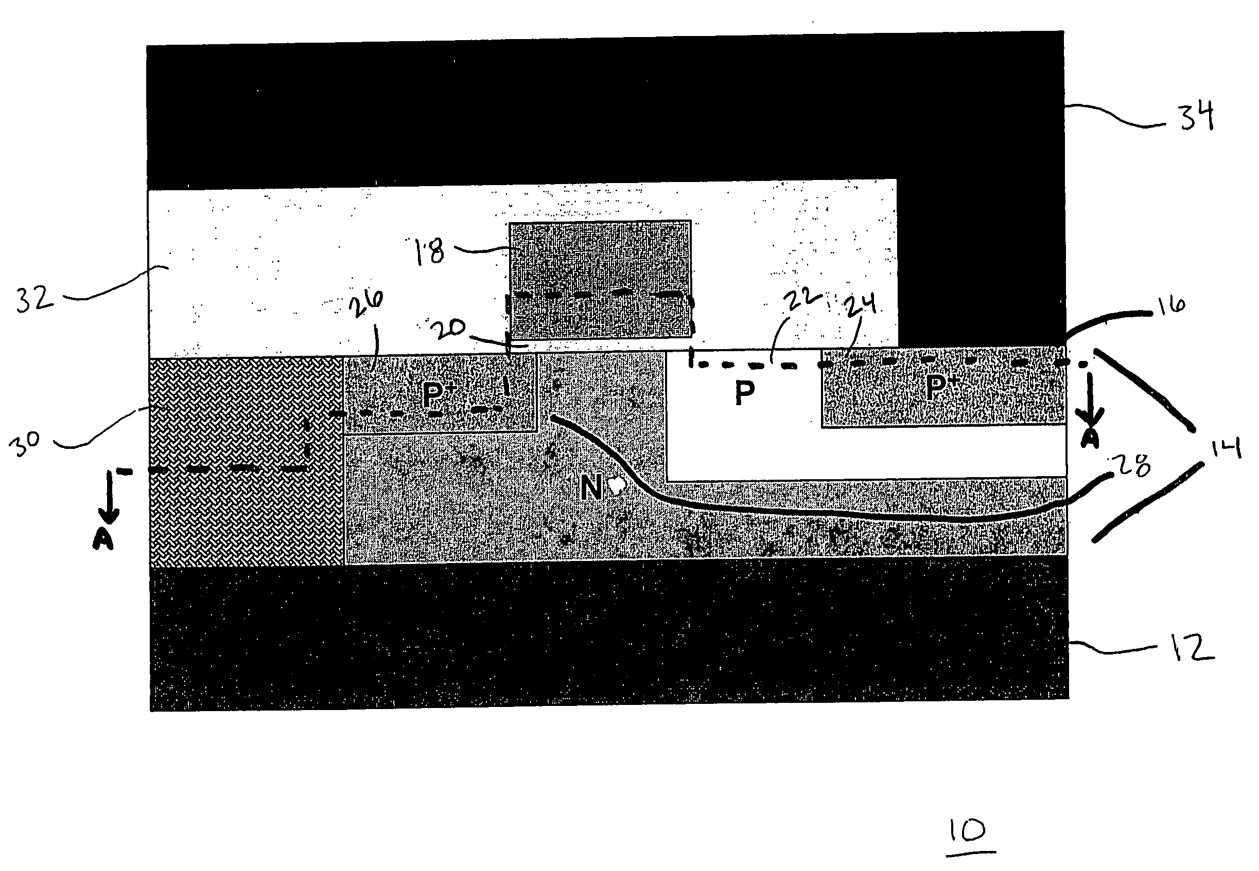
[0025]FIG. 1 is a cross-sectional view of a p-channel LDMOS device with vertical current flow, sometimes referred to herein as a “quasi-vertical LDMOS device.” Device 10 includes a semiconductor substrate or wafer 12, typically a silicon substrate. The silicon substrate 12 is doped to a N+ dopant concentration comprising n-dopants such as phosphorous or arsenic. In an exemplary embodiment, substrate 12 has a thickness of less than 100 μm, and preferably less than about 75 μm (about 3 mils), and most preferably has a thickness equal to about 50 μm (2 m...


PUM


Abstract

A low voltage power device includes a plurality of quasi-vertical LDMOS device cells. A conductive trench sinker is formed through the epitaxial layer and adjacent a selected one of the source and drain regions in each cell. The trench sinker electrically couples the selected one of the source and drain regions to the substrate for coupling current from the channel to the substrate. The resulting device exhibits a vertical current flow between the metal electrode covering the front surface and the second electrode formed at the back side of the wafer. The device cells are arranged in a closed cell configuration.

Description

FIELD OF THE INVENTION [0001] The present invention relates to semiconductor structures and more particularly to lateral double diffused MOS (LDMOS) transistors. BACKGROUND OF THE INVENTION [0002] Power MOSFETs (metal oxide semiconductor (MOS) field effect transistors (FET)) are used as electric switches for high frequency PWM (pulse width modulation) applications such as voltage regulators and as load switches in general power applications. When used as load switches where switching times are usually long, cost, size and on-resistance of the switches are the prevailing design considerations. The primary concern with power devices used as load switches is low specific on resistance (Rds,on* Area). When used in PWM applications, the transistors must exhibit small power loss during switching, which imposes an additional requirement—small internal capacitances—that make the MOSFET design challenging and often times more expensive. [0003] Vertical double diffused MOSFET (VDMOS) having v...

Claims


Application Information

Patent Timeline
Patent Type & Authority Applications(United States)
IPC IPC(8): H01L29/76
CPCH01L29/0692H01L29/0878H01L29/0886H01L29/1045H01L29/7835H01L29/4238H01L29/7802H01L29/7816H01L29/4175
Inventor XU, SHUMINGKOREC, JACEK
Owner CICLON SEMICON DEVICE
Features
  • Generate Ideas
  • Intellectual Property
  • Life Sciences
  • Materials
  • Tech Scout
  • Unparalleled Data Quality
  • Higher Quality Content
  • 60% Fewer Hallucinations
Learn More