Magnetic Field Sensor

a magnetic field and sensor technology, applied in the direction of electrical apparatus construction details, printed circuit non-printed electric components association, instruments, etc., can solve the problems of erroneous operation of the surrounding electronic device or electronic circuit, and achieve the effect of easy design, large electromotive force, and high detection sensitivity

Inactive Publication Date: 2007-09-20
NEC CORP
View PDF2 Cites 24 Cited by
  • Summary
  • Abstract
  • Description
  • Claims
  • Application Information

AI Technical Summary

Benefits of technology

[0016] In the magnetic field sensor according to the present invention, as the number of turns of the stacked coil is larger than 1, the magnetic flux penetrating through the stacked coil increases to be able to induce a comparatively large electromotive force. Hence, even when the stacked coil is downsized, a high detection sensitivity can be maintained. The shape and size of the stacked coil can be easily designed such that the stacked coil can be easily set close to the measurement target object. Therefore, with the magnetic field sensor of the present invention, a high spatial resolution can be achieved easily. As a result, the magnetic field sensor can measure, for example, a high-frequency noise current flowing through a fine electronic circuit easily, and accordingly measures against electromagnetic waves can be easily taken at an early stage of design or the manufacture of an electronic device or electronic circuit.

Problems solved by technology

When an electronic device or electronic circuit emits strong electromagnetic waves, the electromagnetic waves may cause a surrounding electronic device or electronic circuit to operate erroneously.

Method used


Image

  • Magnetic Field Sensor
  • Magnetic Field Sensor
  • Magnetic Field Sensor

Examples


first embodiment

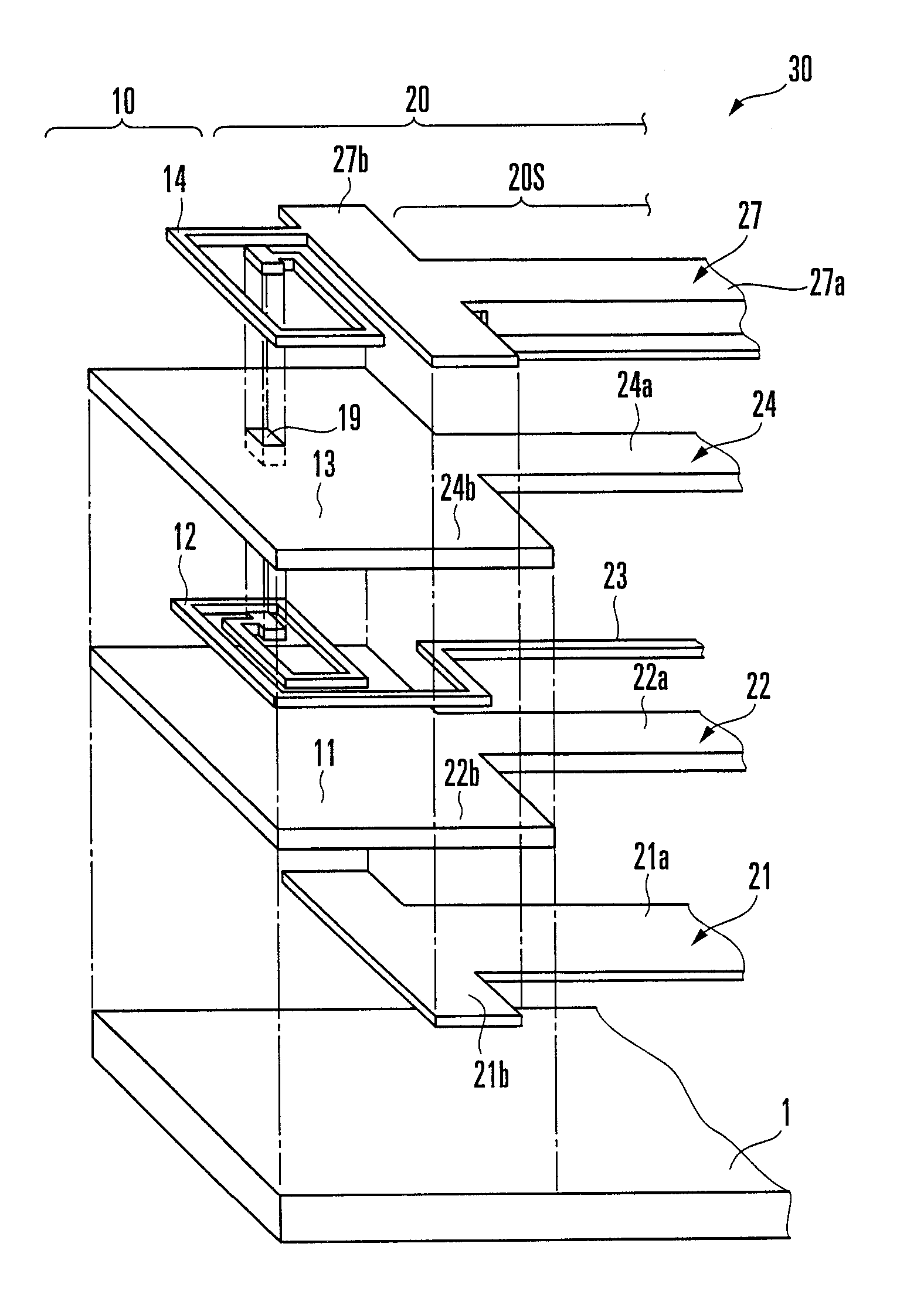
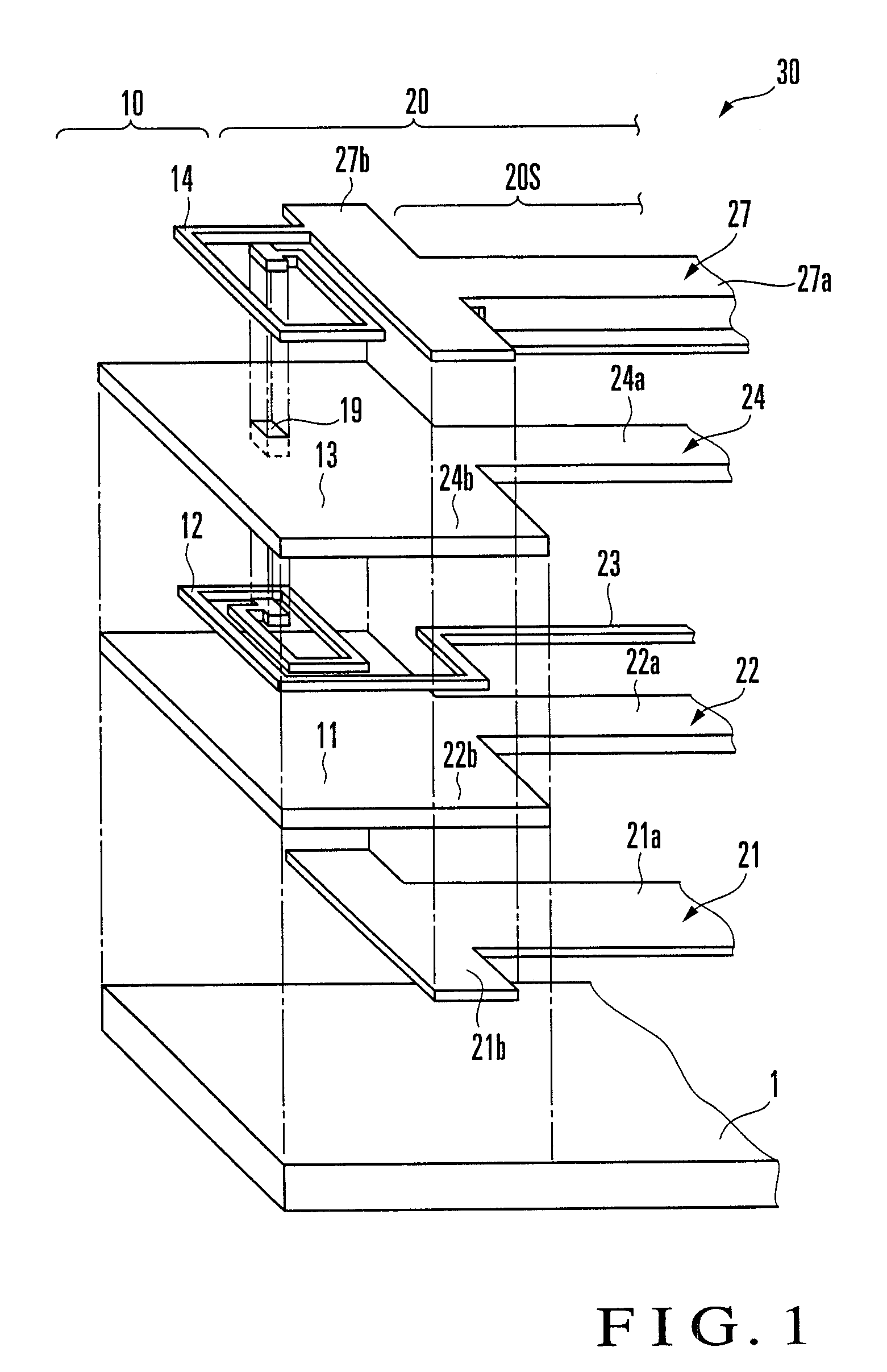
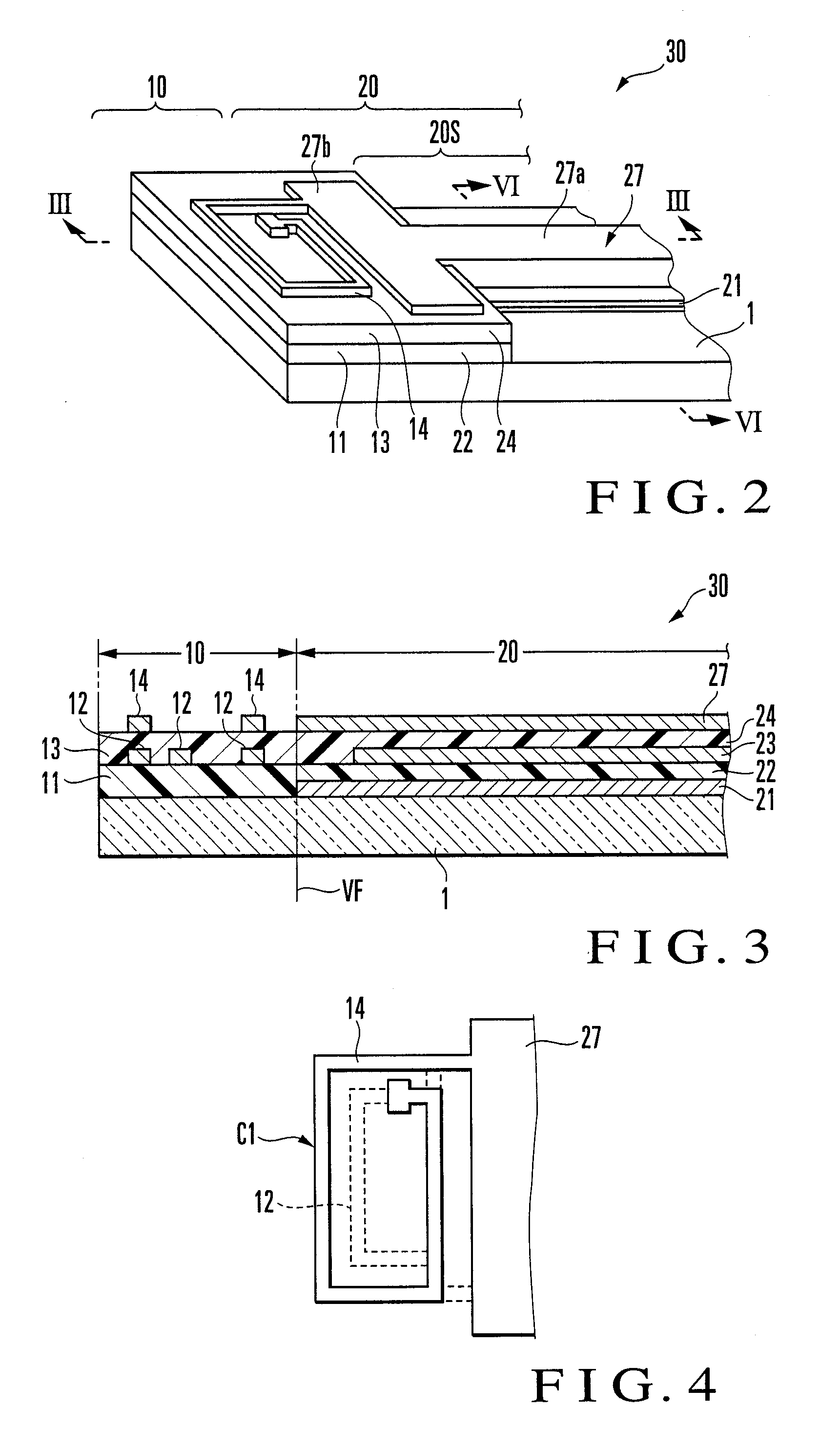
[0044] As shown in FIG. 1, a magnetic field sensor 30 according to the first embodiment of the present invention has a substrate 1, a stacked coil 10 formed on the substrate 1, and a strip line 20 formed on the substrate 1 to continue to the stacked coil 10.

[0045] The stacked coil 10 has a structure in which a coil portion first interlayer dielectric film 11, first coil forming element 12, coil portion second interlayer dielectric film 13, and second coil forming element 14 are stacked on the substrate 1 in the order named. The coil portion second interlayer dielectric film 13 has a contact plug (contact means) 19 which brings the first coil forming element 12 and second coil forming element 14 into contact with each other through a via hole.

[0046] The strip line 20 has a structure in which a lower grounding layer 21, line portion first interlayer dielectric film 22, strip conductor 23, line portion second interlayer dielectric film 24, and upper grounding layer 27 are stacked on ...

second embodiment

[0078] The structure of a magnetic field sensor according to the second embodiment of the present invention is equal to that of the magnetic field sensor 30 of the first embodiment except for the shapes of a first coil forming element 112 and second coil forming element 114. Thus, the overall view of the magnetic field sensor, the exploded perspective views of the respective members, and the sectional structure will be omitted.

[0079] As shown in FIG. 7A, the first coil forming element 112 comprises a coil the number of turns of which is slightly larger than 2.5, and its one end continues to a strip conductor 123. The number of turns of the first coil forming element 112 is larger than that of the magnetic field sensor 30 of the first embodiment described above. Thus, the line width of the first coil forming element 112 is smaller than that of the first coil forming element 12 of the magnetic field sensor 30 of the first embodiment. The line width of the strip conductor 123 is equal...

third embodiment

[0082] As shown in FIG. 8, a magnetic field sensor 230 according to the third embodiment of the present invention is largely different from the magnetic field sensor 30 of the first embodiment in that the entire outer surface of a strip line 220 is formed of a lower grounding layer 221 and upper grounding layer 227, and that the entire strip line 220 forms a shield type strip line region. Except for this, the arrangement of the magnetic field sensor 230 is identical to that of the magnetic field sensor 30 of the first embodiment. Hence, members that are common in function with the constituent members of the magnetic field sensor 30 are denoted by reference numerals formed by adding “200” to the numerical portions of the corresponding reference numerals used in FIGS. 1 and 2, and a description thereof will be omitted.

[0083] In this magnetic field sensor 230, the entire strip line 220 forms the shield type strip line region. Accordingly, the shapes of the respective members excluding...


PUM


Abstract

Two coil forming elements (12, 14) formed of conductor layers and a contact means (19), which is formed in an interlayer dielectric film (13) interposed between the conductor layers and brings the upper and lower coil forming elements into contact with each other through a via hole form a stacked coil (10). One end of the stacked coil is connected to an upper grounding layer (27) of a strip line (20), and the other end of the stacked coil is connected to a strip conductor (23) of the strip line. The number of turns of the stacked coil is larger than 1. A magnetic flux penetrating through the stacked coil increases to be able to induce a relatively large electromotive force. Thus, a high spatial resolution can be obtained easily.

Description

TECHNICAL FIELD [0001] The present invention relates to a magnetic field sensor and, more particularly, to a magnetic field sensor which can detect a high-frequency magnetic field by detecting an electromagnetically induced electromotive force. BACKGROUND ART [0002] Today, the performance and functions in electronic devices improve rapidly. Accordingly, the electromagnetic waves emitted from individual electronic devices or electronic circuits strengthen. When an electronic device or electronic circuit emits strong electromagnetic waves, the electromagnetic waves may cause a surrounding electronic device or electronic circuit to operate erroneously. [0003] As one of factors that cause emission of strong electromagnetic waves, an unwanted high-frequency current flowing through the circuit, particularly a high-frequency noise current flowing through the power supply wiring line of a semiconductor device, is known. To suppress the high-frequency noise current by design or at an early s...

Claims


Application Information

Patent Timeline
Patent Type & Authority Applications(United States)
IPC IPC(8): G01R33/02G01R29/08G01R31/315G01R33/028
CPCG01R29/0878G01R33/028G01R31/315
Inventor ANDO, NORIAKIMASUDA, NORIO
Owner NEC CORP
Why Eureka
Try Eureka