

Method and apparatus for improving uniformity of large-area substrates
a large-area substrate and uniformity technology, applied in the direction of chemical vapor deposition coating, metal material coating process, coating, etc., can solve the problems of increasing the difficulty of achieving uniform film thickness and film property uniformity, and increasing the difficulty of achieving uniform film thickness and film stress uniformity. , to achieve the effect of improving the uniformity of films deposited, and enhancing the effect o
Inactive Publication Date: 2007-09-27
APPLIED MATERIALS INC
View PDF13 Cites 28 Cited by
- Summary
- Abstract
- Description
- Claims
- Application Information
AI Technical Summary
Benefits of technology
[0011]Therefore, there is a need for improved methods and apparatus for improving the uniformity of films deposited on large-area substrates in a plasma enhanced chemical vapor deposition (PECVD) system without affecting the quality of the deposited film.
[0012]Embodiments of the present invention generally provide methods and apparatus for improving the uniformity of a film deposited on a large-area substrate, particularly for films deposited in a PECVD system.
[0013]In one embodiment, a plasma-processing chamber is configured to be asymmetrical relative to a substrate in order to compensate for plasma density non-uniformities in the chamber. In on
Problems solved by technology
As the size of substrates continues to grow, especially when the substrate size is at least about 1300 mm by about 1500 mm (or about 2.0 m2), film thickness uniformity and film property uniformity for large-area, plasma-enhanced chemical vapor deposition (PECVD) becomes more problematic.
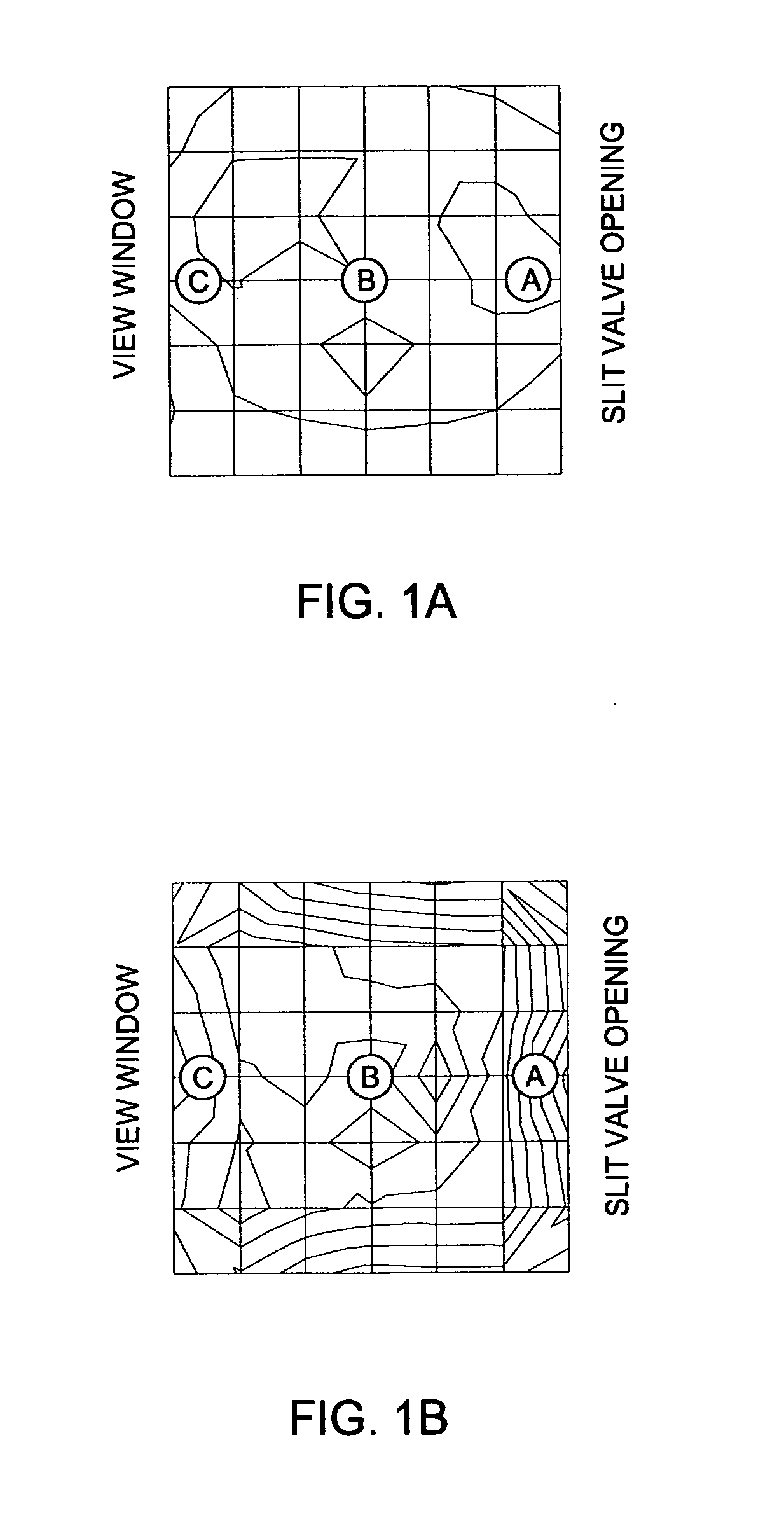
One example of a significant film uniformity problem for large-area substrates occurs during plasma processing
Method used
View moreImage
Smart ImageViewing Examples

Examples
 PUM
| Property | Measurement | Unit |
|---|---|---|
| Fraction | aaaaa | aaaaa |
| Fraction | aaaaa | aaaaa |
| Fraction | aaaaa | aaaaa |
Abstract
Embodiments of the present invention generally provide methods and apparatus for improving the uniformity of a film deposited on a large-area substrate, particularly for films deposited in a PECVD system. In one embodiment, a plasma-processing chamber is configured to be asymmetrical relative to a substrate in order to compensate for plasma density non-uniformities in the chamber caused by unwanted magnetic fields. In another embodiment, a plasma-processing chamber is adapted to create a neutral current bypass path that reduces electric current flow through a magnetic field-generating feature in the chamber. In another embodiment, a method is provided for depositing a uniform film on a large-area substrate in a plasma-processing chamber. The chamber is made electrically symmetric during processing by creating a neutral current bypass path, wherein the neutral current bypass path substantially reduces neutral current flow through a magnetic field-generating feature in the chamber.
Description
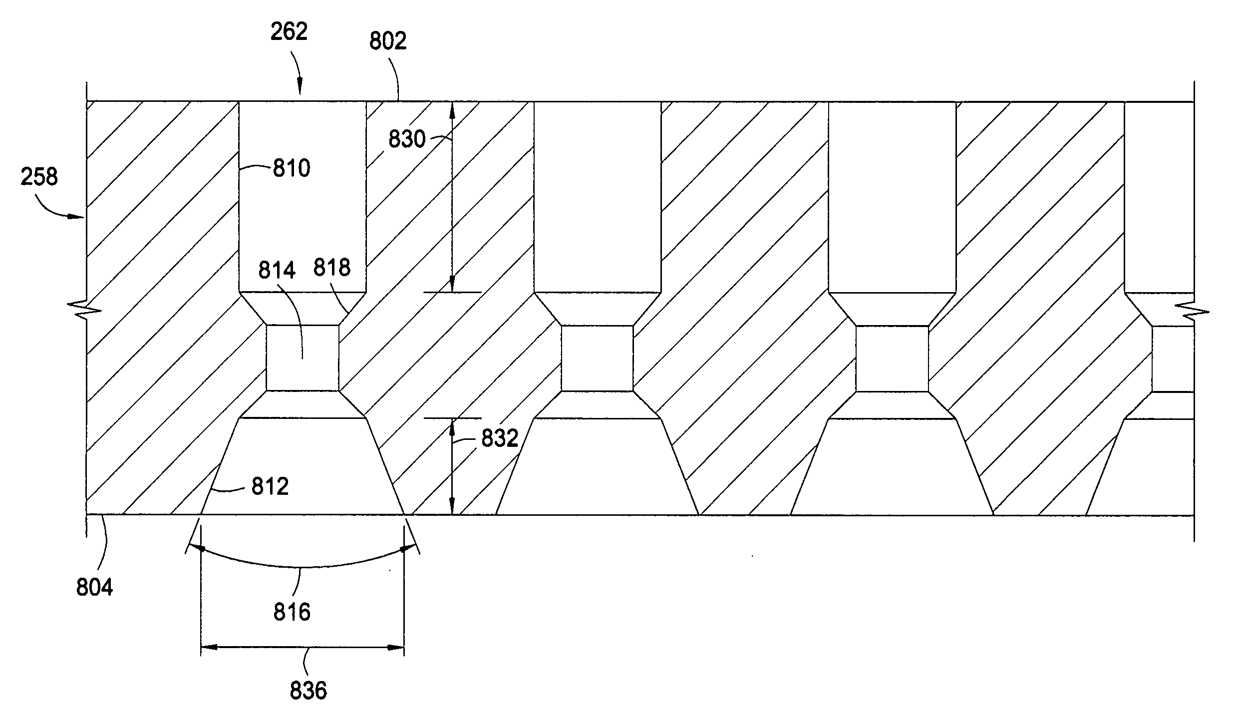
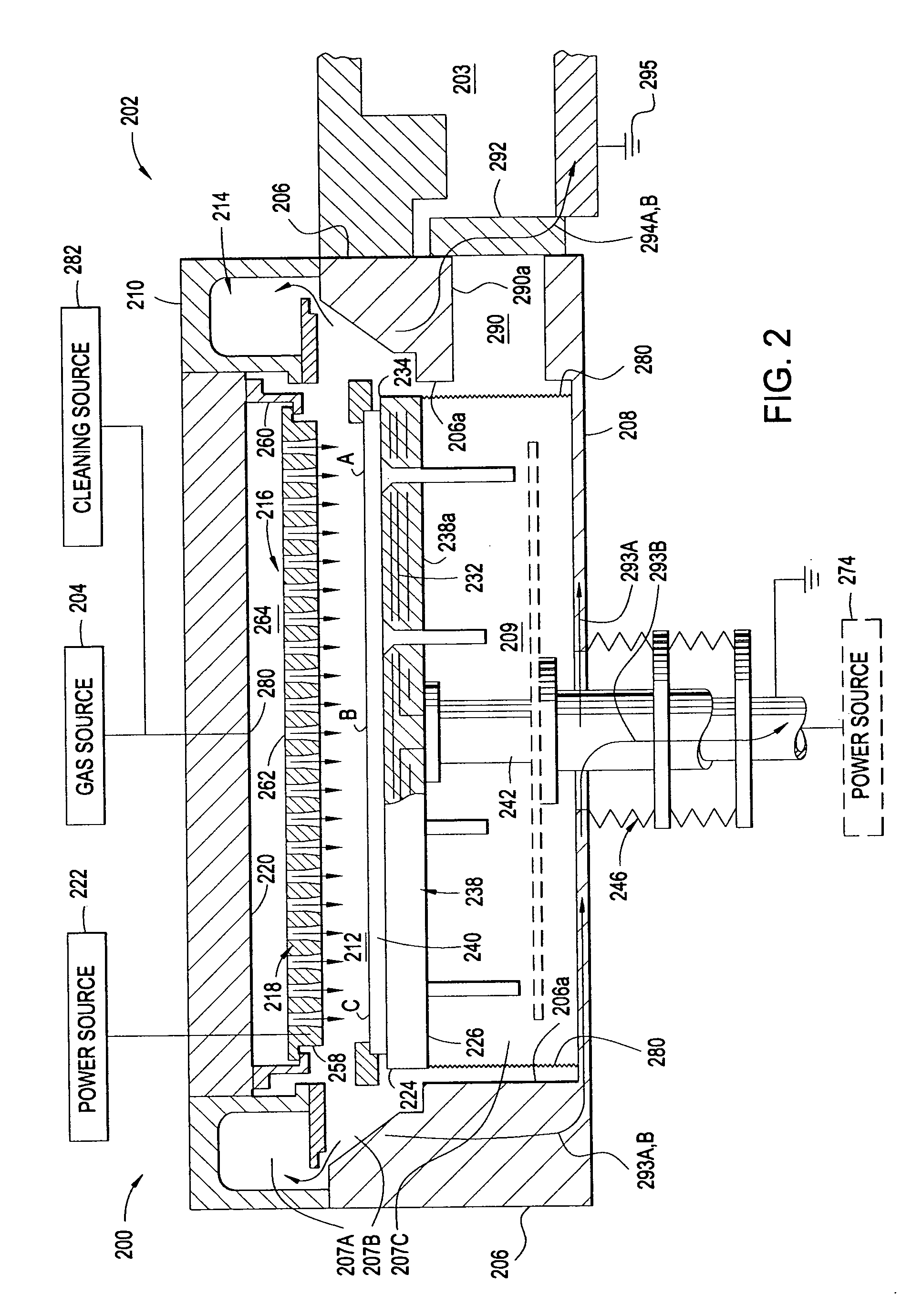
CROSS-REFERENCE TO RELATED APPLICATIONS[0001]This application is a continuation-in-part of co-pending U.S. patent application Ser. No. 11 / 173,210 [APPM 9230.P02], filed Jul. 1, 2005, which is herein incorporated by reference in its entirety to the extent not inconsistent with the claimed invention.BACKGROUND OF THE INVENTION[0002]1. Field of the Invention[0003]Embodiments of the present invention generally relate to deposition of thin films on a large-area substrate.[0004]2. Description of the Related Art[0005]Liquid crystal displays or flat panels are commonly used for active matrix displays such as computer and television monitors. Plasma enhanced chemical vapor deposition (PECVD) is generally employed to deposit thin films on a substrate such as a transparent substrate for flat panel display or semiconductor wafer. PECVD is generally accomplished by introducing a precursor gas or gas mixture into a vacuum chamber that contains a substrate. The precursor gas or gas mixture is typi...
Claims
Login to View More Application Information
Patent Timeline
 IPC IPC(8): C23C16/00
CPCC23C16/345C23C16/52C23C16/5096C23C16/45565C23C16/00C23C16/44
InventorCHOI, SOO YOUNGWHITE, JOHN M.
OwnerAPPLIED MATERIALS INC