Organic light-emitting display substrate, manufacturing method thereof and display device

a technology manufacturing method, which is applied in the field of organic light-emitting display substrate, manufacturing method thereof and display device, can solve the problem that the width of the inkjet printer's inkjet printer cannot be equivalent to the width of the display area, and achieve the effect of improving the overall uniformity of the film layer on the substrate and improving the brightness uniformity of the display devi

Active Publication Date: 2016-12-15
BOE TECH GRP CO LTD
View PDF4 Cites 24 Cited by
  • Summary
  • Abstract
  • Description
  • Claims
  • Application Information

AI Technical Summary

Benefits of technology

[0031]In the present invention, the groove is arranged on the top surface of each dam of the pixel defining layer, and the grooves at least define one frame-shaped area. Before inkjet printing the ink in the frame-shaped areas, a solvent having the same material as the solvent in the ink can be inkjet printed in the grooves first. Therefore, when the ink is inkjet printed in the frame-shaped areas defined by the grooves, since the material of the solvent accommodated in the grooves is the same as that of the solvent in the ink, the ambience at the boundaries of the frame-shaped areas is the same as that in the interior thereof, and then the thickness and the density of the film layer formed in the frame-shaped areas after the solvent in the ink is evaporated are more uniform. Accordingly, the overall uniformity of the film layer on the substrate is improved, and the brightness uniformity of the display device is improved.

Problems solved by technology

With regard to equipment including a large-sized organic light emitting display device, generally the size of an inkjet head for inkjet printing cannot be equivalent to the width of a display area due to technical limits.

Method used


Image

  • Organic light-emitting display substrate, manufacturing method thereof and display device
  • Organic light-emitting display substrate, manufacturing method thereof and display device
  • Organic light-emitting display substrate, manufacturing method thereof and display device

Examples


Embodiment Construction

[0038]The specific embodiments of the present invention will be illustrated below in detail in conjunction with the accompany drawings. It should be understood that the specific embodiments described herein are merely used for illustrating and explaining the present invention, rather than limiting the present invention.

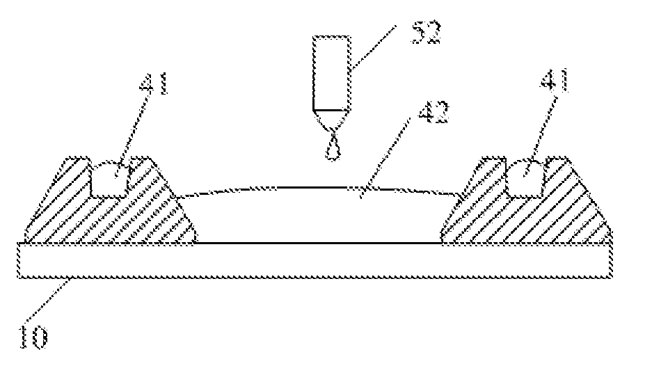
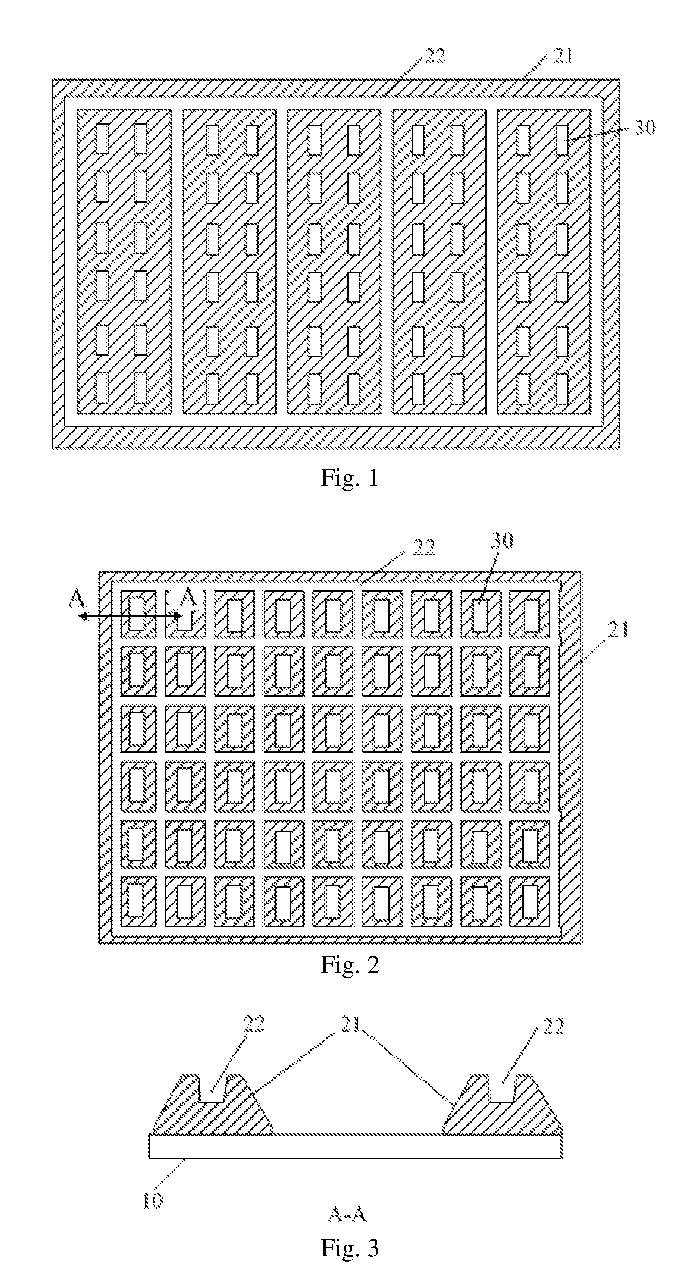
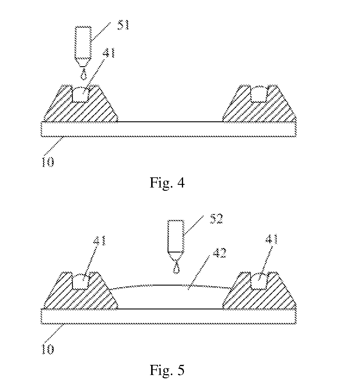
[0039]As one aspect of the present invention, provided is an organic light-emitting display substrate, as shown in FIG. 1, including a substrate 10 and a pixel defining layer arranged on the substrate 10, the pixel defining layer including a plurality of dams 21 crisscrossing in a display area of the organic light-emitting display substrate, the dams 21 crisscrossing to define a plurality of pixel units and define the boundary of the display area, wherein the pixel defining layer further includes a groove 22 arranged on a top surface of each dam 21, the grooves 22 at least define one frame-shaped area, at least one pixel unit 30 is arranged in each frame-shaped area, ...


PUM


Abstract

Disclosed is an organic light-emitting display substrate, including a substrate and a pixel defining layer on the substrate which includes a plurality of dams crisscrossing in a display area of the substrate to define a plurality of pixel units and define the boundary of the display area, wherein the pixel defining layer further includes a groove arranged on a top surface of each dam, the grooves at least define one frame-shaped area, at least one pixel unit is arranged in each frame-shaped area, and the grooves are used for accommodating a solvent when forming an organic light-emitting element by inkjet printing. Also disclosed is a manufacturing method of an organic light-emitting display substrate and a display device. The present invention can improve the film forming effect of a film layer formed on the substrate, so that the brightness of a display image of the display device is more uniform.

Description

FIELD OF THE INVENTION[0001]The present invention relates to the field of display technology, and in particular, to an organic light-emitting display substrate, a manufacturing method thereof and a display device.BACKGROUND OF THE INVENTION[0002]An organic light-emitting display substrate includes a substrate, and an anode electrode layer, a light emitting functional layer and a cathode electrode layer which are arranged on the substrate. In a manufacturing process of an organic light-emitting display substrate, a light emitting functional layer can be formed on an anode electrode layer by inkjet printing. Considering the fluidity of ink, a pixel defining layer is generally arranged in non-pixel areas between the pixel pattern areas in order to reduce overflow of the ink for inkjet printing to adjacent pixel pattern areas. The pixel defining layer is provided with a plurality of openings corresponding to pixel units, and light emitting functional layer ink is spray coated in the ope...

Claims


Application Information

Patent Timeline
Patent Type & Authority Applications(United States)
IPC IPC(8): H01L27/32H01L51/00H01L51/56
CPCH01L27/3246H01L51/0005H01L51/56H10K71/135H10K59/122H10K71/00
Inventor JIAO, ZHIQIANGHOU, WENJUNLIAO, CHINLUNG
Owner BOE TECH GRP CO LTD
Why Eureka
Try Eureka