Systems and methods for depositing patterned materials for solar panel production

Inactive Publication Date: 2010-07-22
ALION
View PDF98 Cites 25 Cited by
  • Summary
  • Abstract
  • Description
  • Claims
  • Application Information

AI Technical Summary

Benefits of technology

[0014]Many benefits are achieved by way of the present invention over conventional techniques. Certain embodiments of the present invention can improve film uniformity and/or edge definition in thin films for photovoltaic modules. Some embodiments of the present invention can improve material patterns for photovoltaic modules and/or cells. Certain embodiments of the present invention implement an optical feedback system to det

Problems solved by technology

However, the production of photovoltaics is limited by the high cost of fabricating such devices.
Conventional manufacturing techniques for thin film photovoltaic devices are expensive.
Most of these techniques require vacuum environments which drastically increase the capital cost, maintenance cost, and material cost required to manufacture thin film photovoltaic devices.
Furthermore, these conventional techniques generally have very poor material use efficiency, as they often deposit material non-specifically inside a deposition chamber, thereby significantly increasing the total cost of the photovoltaic module.
In addition, as these methods usually deposit material over the entire substrate, the layers often need subsequent partitioning or scribing into a series of interconnected cells to produce a photovoltaic module.
Partitioning or scribing is relatively slow, expensive, prone to yield problems, and wasteful of the material between cells and near the module edges.
On the other hand, many printing techniques exist, yet each has its own drawbacks for the manufacture of thin film photovoltaic modules.
For example, conventional screen printing can be low cost, but often is difficult to align precisely over large areas, and can result in layers with a minimum thickness of 10 microns (high material use), with poor resultant lay

Method used


Image

  • Systems and methods for depositing patterned materials for solar panel production
  • Systems and methods for depositing patterned materials for solar panel production
  • Systems and methods for depositing patterned materials for solar panel production

Examples


Embodiment Construction

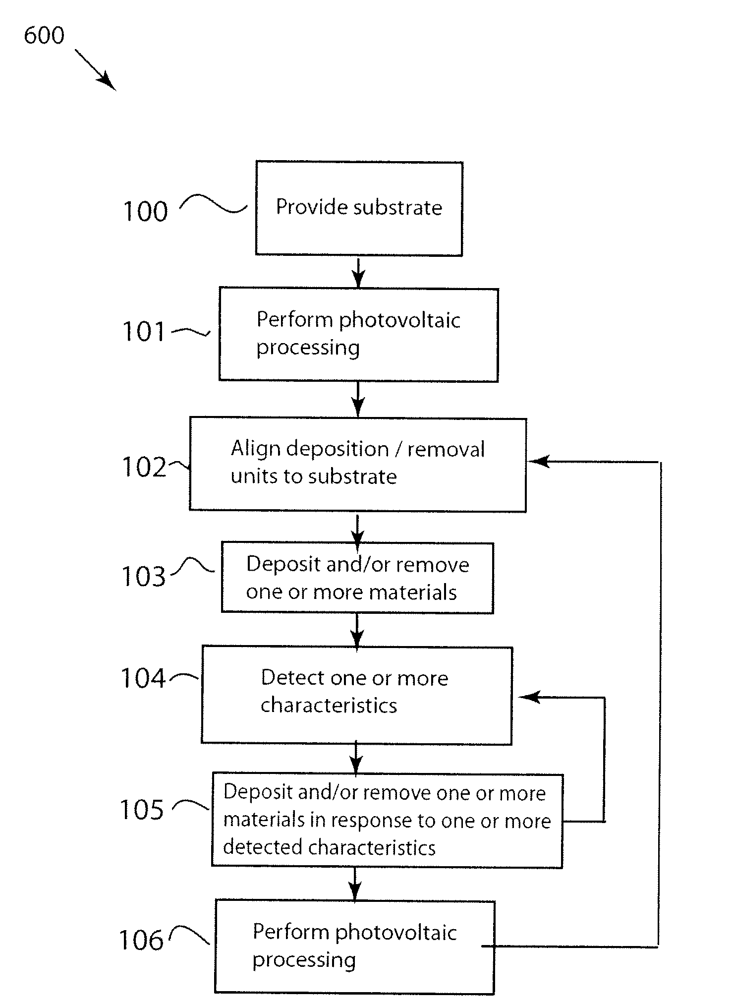
[0022]The present invention is directed to material deposition. More particularly, the invention provides systems and methods for depositing material with predetermined characteristics. Merely by way of example, the invention has been applied to making photovoltaic devices. But it would be recognized that the invention has a much broader range of applicability.

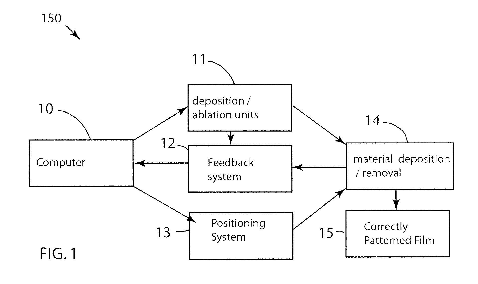
[0023]FIG. 1 is a simplified diagram showing a method for depositing one or more materials for photovoltaic cells according to one embodiment of the present invention. This diagram is merely an example, which should not unduly limit the scope of the claims. One of ordinary skill in the art would recognize many variations, alternatives, and modifications.

[0024]For example, the method 150 as shown in FIG. 1 deposits the one or more materials with or without predetermined patterns. In another example, the method 150 uses a feedback to detect film defects, and / or uses one or more deposition and / or removal processes to repair these...


PUM


Abstract

Method and system for forming one or more predetermined patterns on a substrate for making a photovoltaic device. The method includes aligning at least a first droplet source with a substrate, dispensing one or more first droplets associated with one or more first materials from the first droplet source, and forming at least a first pattern of one or more second materials on the substrate by at least the first droplet source. Additionally, the method includes providing a first light beam incident on at least the first pattern, obtaining a first signal associated with the first pattern in response to the first light beam, processing information associated with the first signal, and determining one or more first characteristics of the first pattern based on at least information associated with the first signal.

Description

1. CROSS-REFERENCES TO RELATED APPLICATIONS[0001]This application claims priority to U.S. Provisional No. 61 / 205,545, filed Jan. 20, 2009, commonly assigned, incorporated by reference herein for all purposes.[0002]Additionally, this application is related to U.S. patent application Ser. No. 12 / 329,325, commonly assigned, incorporated by reference herein for all purposes.2. BACKGROUND OF THE INVENTION[0003]The present invention is directed to material deposition. More particularly, the invention provides systems and methods for depositing material with predetermined characteristics. Merely by way of example, the invention has been applied to making photovoltaic devices. But it would be recognized that the invention has a much broader range of applicability.[0004]Photovoltaics convert sunlight into electricity, providing a desirable source of clean energy. Some examples of current commercial photovoltaic solar cells are made of crystalline silicon and thin film (CdTe (Cadmium Tellurid...

Claims


Application Information

Patent Timeline
IPC IPC(8): H01L31/18H01L21/04
CPCB41J2/16579H01L31/022425H01L31/022466H01L31/18Y02P70/521H01L51/0005H01L51/4253Y02E10/549H01L31/1836Y02P70/50H10K71/135H10K30/30
Inventor HUNT, THOMAS PETER
Owner ALION
Why Eureka
Try Eureka