Semiconductor device and method of fabricating the same

a technology of semiconductors and transistors, applied in the field of semiconductor devices, can solve the problems of inability to obtain a large thickness of ge layer, inability to design a large degree of freedom, and insufficient current driving force of the finfet, etc., and achieve the effect of increasing the ge concentration of the fin

Inactive Publication Date: 2007-09-27
KK TOSHIBA
View PDF6 Cites 324 Cited by
  • Summary
  • Abstract
  • Description
  • Claims
  • Application Information

AI Technical Summary

Benefits of technology

[0019]oxidizing surfaces of the buffer layer and the SiGe layer of the fin

Problems solved by technology

However, although according to the technique described in the non-patent literary document, the planar type FET can be relatively, simply formed, a problem is caused when a FinFET having a Ge-channel or SiGe-channel is supposed.
Thus, since a fin height of the FinFET, that is, a maximum channel width of the FinFET depends on the thicknes

Method used


Image

  • Semiconductor device and method of fabricating the same
  • Semiconductor device and method of fabricating the same
  • Semiconductor device and method of fabricating the same

Examples


first embodiment

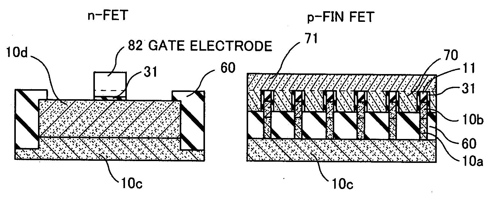
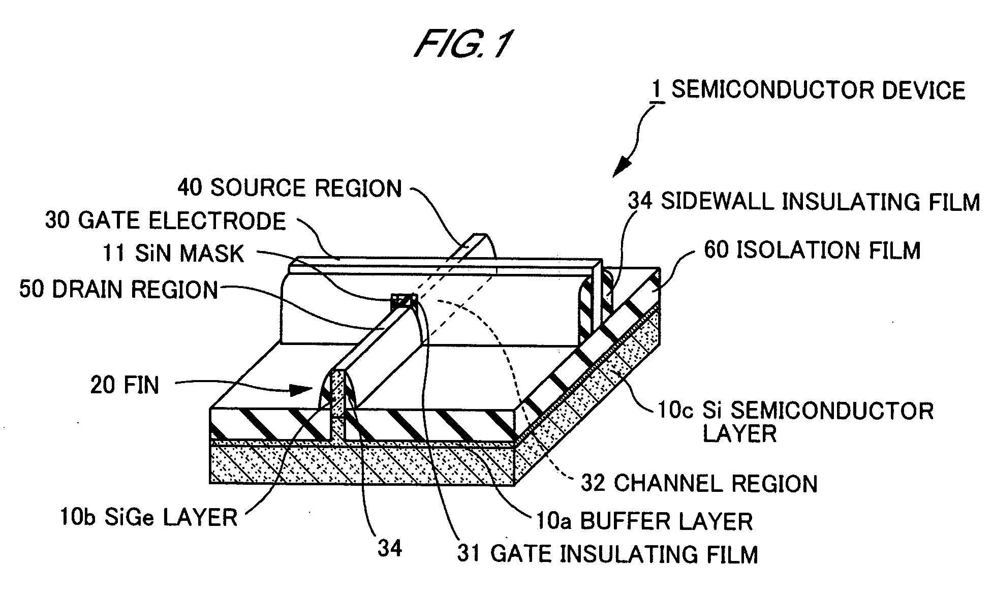
[0030]FIG. 1 is a perspective view showing a structure of a p-channel FinFET (hereinafter referred to as “a p-FinFET”) as a semiconductor device according to the present invention.

[0031]A p-FinFET has a fin 20 including a source region 40 and a drain region 50 each of which is formed to have a predetermined height, and a gate electrode 30. Elements are isolated from one another through an isolation film 60.

[0032]A thickness of the fin 20, for example, is 20 nm and a height of the fin 20, for example, is in the range of 50 to 100 nm. The fin 20 has a buffer layer 10a formed on a Si layer 10c, and a SiGe layer 10b formed on the buffer layer 10a.

[0033]The buffer layer 10a is made of SiGe, and a Ge concentration of the buffer layer 10a gradually increases substantially along a height direction of the fin 20.

[0034]The SiGe layer 10b has a nearly uniform Ge concentration corresponding to the Ge concentration of the buffer layer 10a in an interface between the SiGe layer 10b and the buffe...

second embodiment

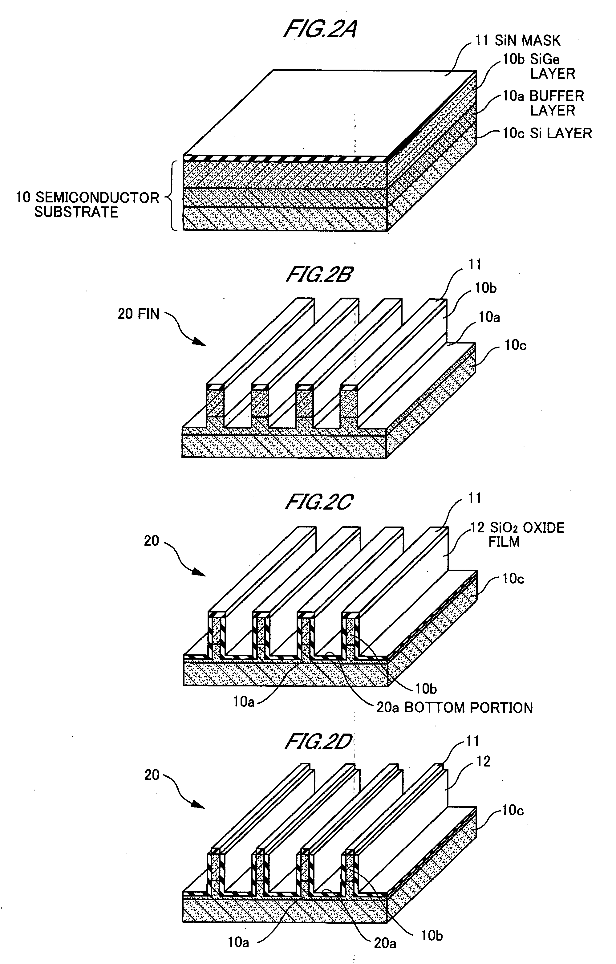
[0062]FIGS. 3A to 3C are respectively perspective views showing processes for fabricating a p-FinFET according to the present invention.

[0063](2a) An SGOI substrate is prepared which is formed by laminating a buried oxide (BOX) layer 110d, a Si layer 100c, a buffer layer 100a, and a SiGe layer 100b in order on a Si substrate 100. In addition, a SiN mask 11 is formed on the SiGe layer 100b (FIG. 3A).

[0064]A SiGe crystal is epitaxially grown while a concentration of Ge contained in the SiGe crystal is gradually grown from an interface between the Si layer 100c and the SiGe crystal to an interface between the SiGe layer 100b and the SiGe crystal in order to alleviate the lattice mismatch, thereby forming the buffer layer 100a.

[0065]The SiGe layer 100b has a nearly uniform Ge concentration corresponding to a Ge concentration of the buffer layer 100a in the interface between the SiGe layer 100b and the buffer layer 100a, and preferably has nearly the same Ge concentration as that of the...

third embodiment

[0073]FIGS. 4A to 4K are respectively cross sectional views showing processes for fabricating an n-FinFET and a p-FinFET according to the present invention. In these figures, processes for fabricating an n-FinFET region in respective stages are shown on a left-hand side, and processes for fabricating a p-FinFET region in respective stages are shown on a right-hand side.

[0074](3a) A buffer layer 10a is formed on a Si layer 10c by utilizing the CVD method, and a SiGe layer 10b is formed on the buffer layer 10a. After that, a SiN mask 11 is formed on the SiGe layer 10b (FIG. 4A).

[0075]A SiGe crystal is epitaxially grown while a concentration of Ge contained in the SiGe crystal is gradually increased from an interface between the Si layer 10c and the SiGe crystal to an interface between the SiGe layer 10b and the SiGe crystal in order to alleviate the lattice mismatch, thereby forming the buffer layer 10a.

[0076]The SiGe layer 10b has a nearly uniform Ge concentration corresponding to a...


PUM


Abstract

A semiconductor device according to one embodiment of the present invention includes: a fin including a buffer layer made of SiGe and formed on a Si layer, and a SiGe layer formed on the buffer layer, the SiGe layer having a Ge concentration corresponding to a Ge concentration of the buffer layer in an interface between the buffer layer and the SiGe layer; a gate electrode formed on a side face of the fin through a gate insulating film; a channel region formed in a region within the fin facing the gate electrode through the gate insulating film, the channel region being selectively provided within the SiGe layer of the buffer layer and the SiGe layer included in the fin; and a source region and a drain region formed within the fin, the channel region being formed between the source region and the drain region.

Description

CROSS-REFERENCE TO RELATED APPLICATIONS[0001]This application is based upon and claims the benefit of priority from prior Japanese Patent Application No. 2006-081559, filed Mar. 23, 2006, the entire contents of which are incorporated herein by reference.BACKGROUND OF THE INVENTION[0002]The present invention relates to a semiconductor device and a method of fabricating the same, and more particularly to a device structure of a fin-field effect transistor (FinFET) and a method of fabricating the FinFET.[0003]In recent years, in LSIs formed on silicon substrates, the high performance promotion has been attained through scale down of elements used in the LSIs. A gate length is shortened and a gate insulating film is thinned in accordance with a so-called scaling law in a MOSFET used in a logic circuit, or a memory such as an SRAM, which results in the high performance promotion being realized in the LSIs. At present, in order to improve cutoff characteristics in a short channel region h...

Claims


Application Information

Patent Timeline
IPC IPC(8): H01L31/00
CPCH01L21/823807H01L21/823814H01L21/823821H01L21/823828H01L29/78687H01L27/1211H01L29/1054H01L29/66795H01L29/785H01L21/823878
Inventor INABA, SATOSHI
Owner KK TOSHIBA
Why Eureka
Try Eureka