Nonvolatile semiconductor memory device and method for manufacturing same
a semiconductor memory and non-volatile technology, applied in the direction of semiconductor devices, electrical devices, transistors, etc., can solve the problems of deteriorating electrical characteristics and variation of threshold voltag
- Summary
- Abstract
- Description
- Claims
- Application Information
AI Technical Summary
Benefits of technology
Problems solved by technology
Method used
Image
Examples
first embodiment
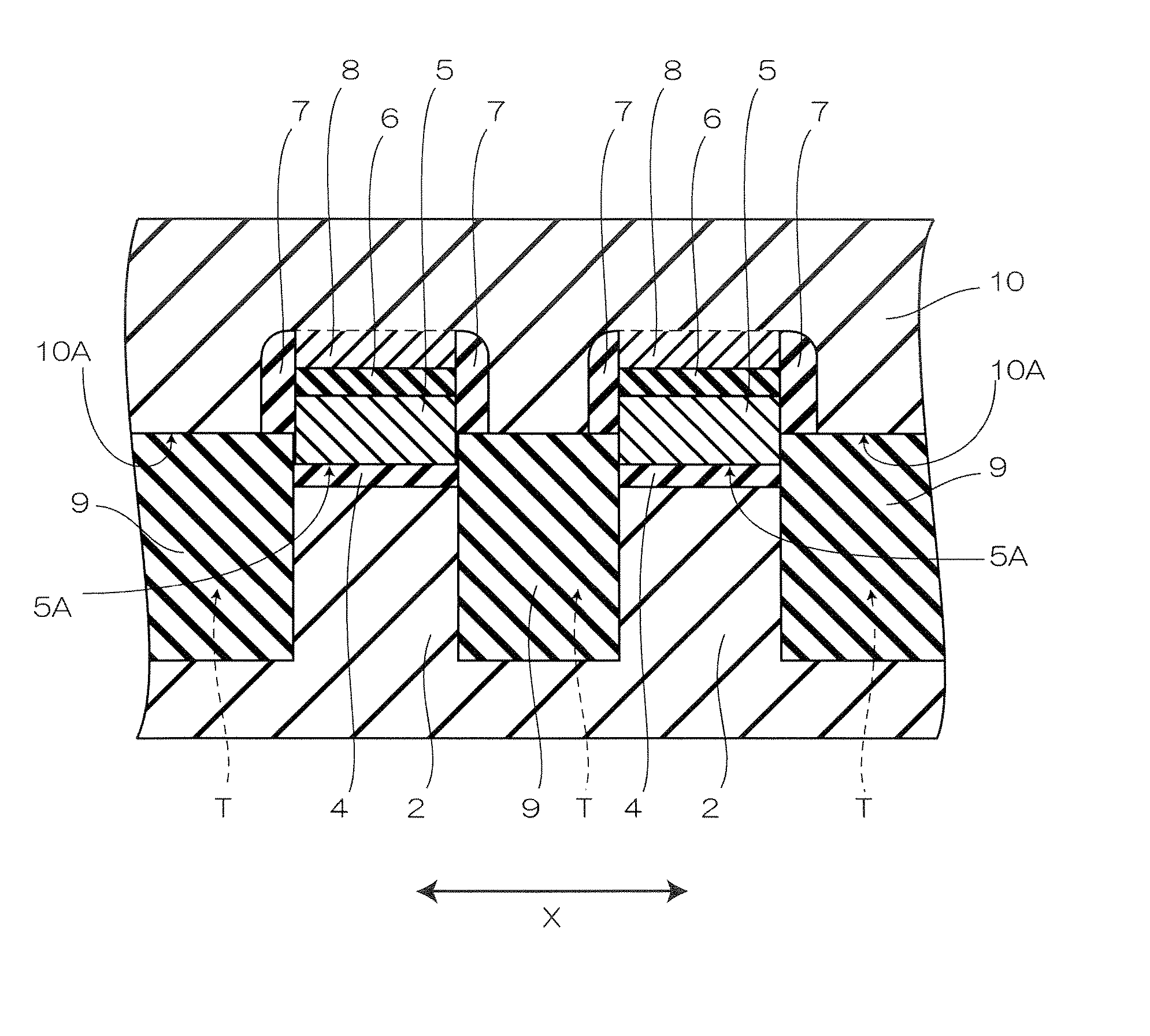
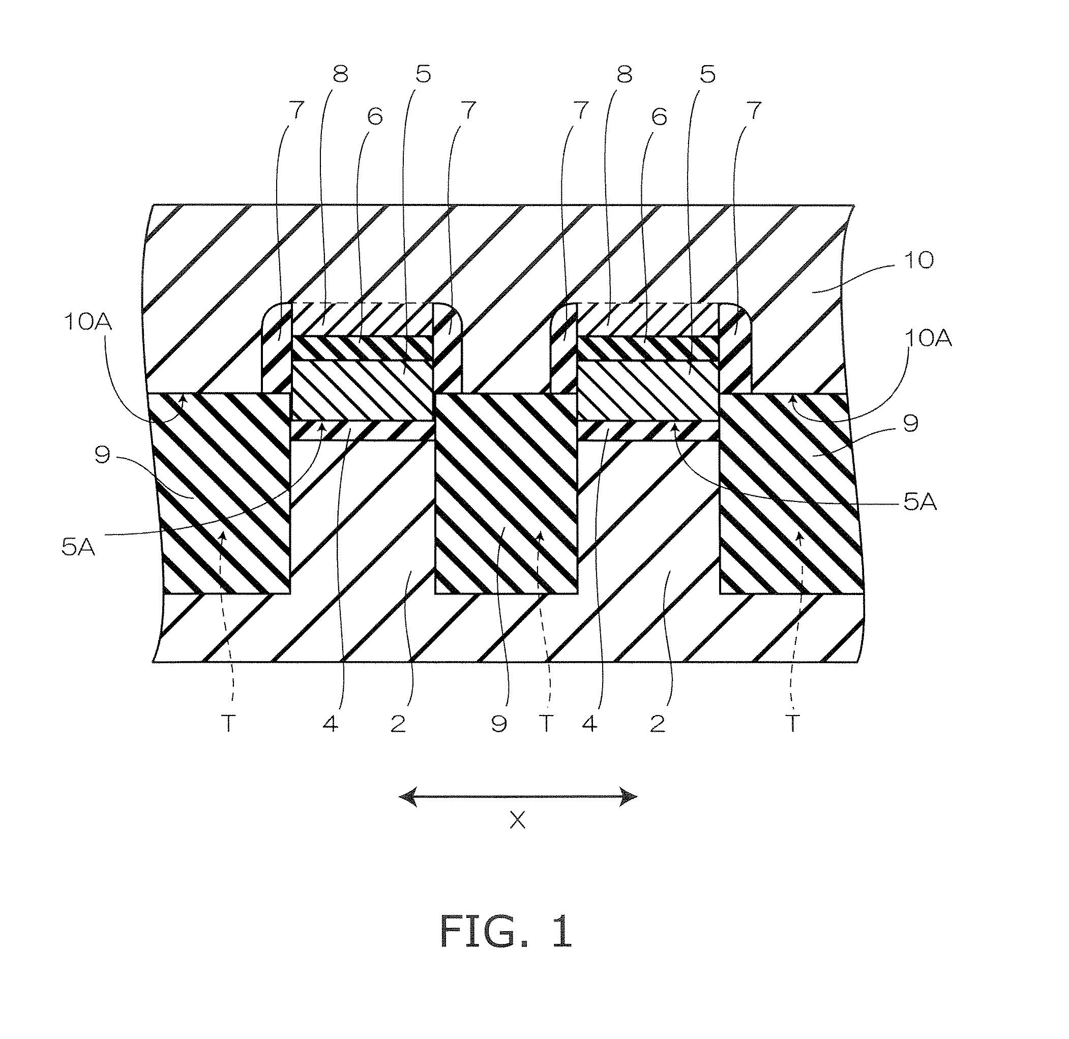
[0024]FIG. 1 is a schematic cross-sectional view illustrating the cross-sectional structure of the main part of a nonvolatile semiconductor memory device according to a first embodiment of the invention.
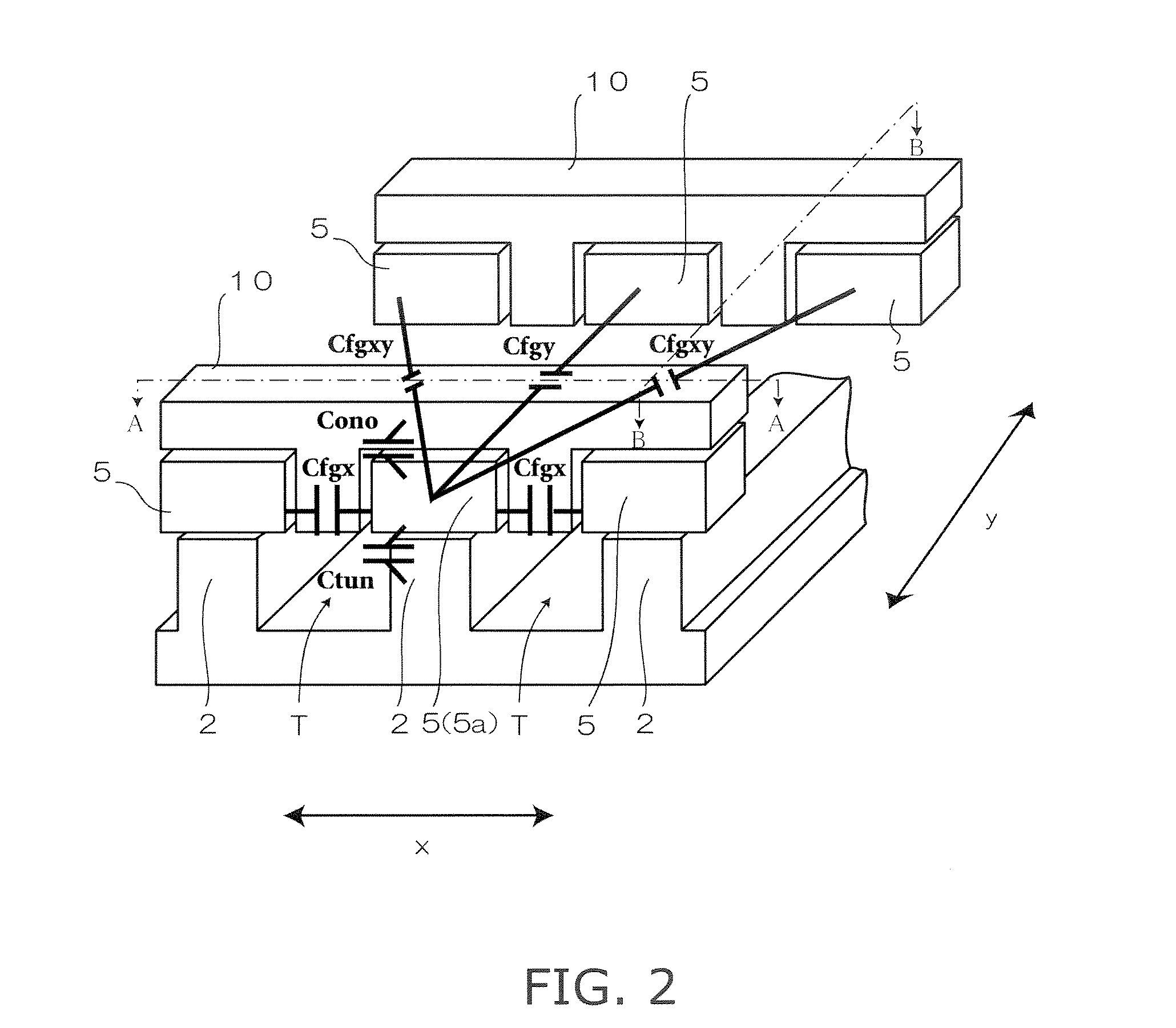
[0025] In this embodiment, by forming trenches T in a silicon substrate, a plurality of semiconductor layers 2 spaced from each other and arranged in a first direction x are formed. Each semiconductor layer 2 extends in a second direction y (the direction through the page in FIG. 1) substantially orthogonal to the first direction x. In the surface portion of the semiconductor layer 2, a source region and a drain region are formed, which are spaced in the second direction.
[0026] A gate insulating film (tunnel insulating film) 4 is provided on the semiconductor layer 2. A floating gate electrode 5 is provided on the gate insulating film 4. The floating gate electrode 5 is illustratively made of polycrystalline silicon. The trench T is filled inside with a device isolation insulating ...
second embodiment
[0066]FIG. 14 is a schematic view illustrating the cross-sectional structure of the main part of a nonvolatile semiconductor memory device according to a second embodiment of the invention.
[0067] In this embodiment, no polycrystalline silicon layer 8 is provided on the first dielectric film 6. More specifically, without forming a polycrystalline silicon layer 8 on the first dielectric film 6 in FIG. 9, a process as shown in FIGS. 9 to 11 is conducted. Then, as shown in FIG. 15, a second dielectric film 7 is deposited on the device isolation insulating layer 9 so as to cover part of the floating gate electrode 5 protruding upward from the device isolation insulating layer 9 and the first dielectric film 6. Then the second dielectric film 7 on the first dielectric film 6 and on the device isolation insulating layer 9 is etched by RIE to leave the second dielectric film 7 only on the side face of part of the floating gate electrode 5 protruding upward from the device isolation insulat...
third embodiment
[0069]FIG. 16 is a schematic view illustrating the cross-sectional structure of the main part of a nonvolatile semiconductor memory device according to a third embodiment of the invention.
[0070] In this embodiment, the second dielectric film 7 on the polycrystalline silicon layer 8 is removed by CMP. Thus the second dielectric film 7 is left on the entire surface of the device isolation insulating layer 9.
PUM
 Abstract
Description
Claims
Application Information


