Method for manufacturing semiconductor device

a semiconductor integrated circuit and manufacturing method technology, applied in the field of semiconductor integrated circuit manufacturing methods, can solve the problems of signal delay, poor mechanical strength of the film, and deterioration of the adhesive between an upper layer and an underlying layer,

Inactive Publication Date: 2005-08-04
ROHM CO LTD
View PDF9 Cites 8 Cited by
  • Summary
  • Abstract
  • Description
  • Claims
  • Application Information

AI Technical Summary

Benefits of technology

[0011] Note that the term “low dielectric constant material” as used in this specification means materials having relative dielectric constants lower than that of conventional silicon oxide (SiO2), and more specifically, means materials having relative dielectric constants lower than 4.

Problems solved by technology

Metallic wiring in a semiconductor integrated circuit has encountered a significant problem of signal delay due to the increase of wiring resistance and interwiring capacitance as the wiring pitch decreases.
However, since the low dielectric constant (low-k) film is formed as porous material in many cases, a mechanical strength of the film becomes poor and, also, adhesiveness between an upper layer and an underlying layer tends to be deteriorated.
This problem provokes a fall of reliability due to film peeling and moisture penetration at interfaces in subsequent processes.
Moreover, void may be generated along interfaces inside the film due to low adhesiveness in the low dielectric constant film having porosities.
However, the adhesiveness can not be improved sufficiently by above structure.

Method used


Image

  • Method for manufacturing semiconductor device
  • Method for manufacturing semiconductor device
  • Method for manufacturing semiconductor device

Examples


Embodiment Construction

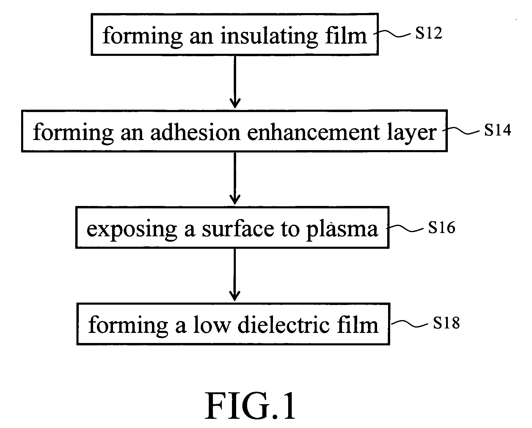
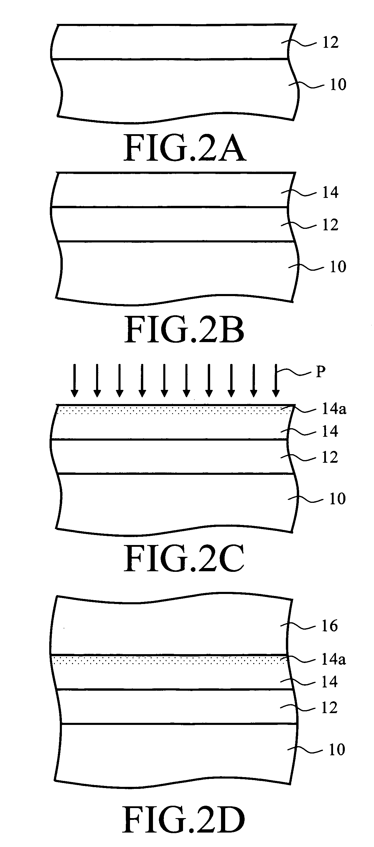
[0021] Referring to drawings, some embodiments of the present invention will now be described in detail. FIG. 1 is a flow chart showing the method for manufacturing a semiconductor device according to the present embodiment. FIGS. 2A through 2D are process cross-sectional views showing a principal part of the manufacturing method according to the present embodiment.

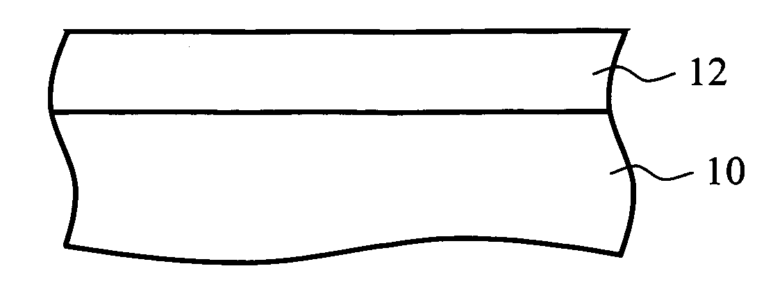
[0022] First, as shown in FIG. 1 (step S12) and FIG. 2A, an insulating film 12 is formed on a substrate 10. A semiconductor substrate on which a predetermined semiconductor element is formed can be used as the substrate 10, for example, as explained later in detail referring to an example.

[0023] The insulating film 12 can be made of materials appropriately selected according to various uses, such as a low dielectric constant film, an etching stopper, a buffer layer, and a hard mask. For example, when the insulating film 12 is used as the etching stopper, the insulating film 12 maybe made of the thin film including silic...


PUM

PropertyMeasurementUnit
relative dielectric constantaaaaaaaaaa
dielectric constantsaaaaaaaaaa
timeaaaaaaaaaa

Abstract

A method for manufacturing a semiconductor device comprises: exposing a surface of a substrate to plasma; and forming an insulating film containing a low dielectric constant material on the surface of the substrate. A method for manufacturing a semiconductor device comprises: forming a modified layer by exposing a surface of a substrate to plasma; and forming an insulating film containing a low dielectric constant material on the modified layer. A method for manufacturing a semiconductor device comprises: forming an adhesion enhancement layer on a substrate; exposing a surface of the adhesion enhancement layer to plasma; and forming a first insulating film on the adhesion enhancement layer.

Description

CROSS-REFERENCE TO RELATED APPLICATIONS [0001] This application is based upon and claims the benefit of priority from the prior Japanese Patent Application No. 2004-021341, filed on Jan. 29, 2004; the entire contents of which are incorporated herein by reference. BACKGROUND OF THE INVENTION [0002] The invention relates to a method for manufacturing a semiconductor device, and more particularly, to a method for manufacturing a semiconductor device with an interlayer insulating structure using low dielectric constant insulating film and a method of manufacturing the same. [0003] Metallic wiring in a semiconductor integrated circuit has encountered a significant problem of signal delay due to the increase of wiring resistance and interwiring capacitance as the wiring pitch decreases. To solve this, the reduction of dielectric constant of the interlayer isolation film provided between the wirings is indispensable (see, e.g., Japanese Laid-Open Patent Application H11-97533 (1999)). For e...

Claims


Application Information

Patent Timeline
Patent Type & Authority Applications(United States)
IPC IPC(8): H01L21/312H01L21/316H01L21/768H05H1/00
CPCH01L21/02137H01L21/02282H01L21/02304H01L21/02315H01L21/76835H01L21/76826H01L21/76829H01L21/76832H01L21/31633
Inventor MATSUMOTO, ISAOOHASHI, NAOFUMIMISAWA, KAORISONE, SHUJI
Owner ROHM CO LTD
Why Eureka
Try Eureka