Nanocontacts having improved contact shape

a technology of nanocontacts and contact shapes, applied in nanoinformatics, instruments, record information storage, etc., can solve the problems of device reliability degradation and very fast operation speed

Inactive Publication Date: 2007-09-27
KOREA CHUNGANG EDUCATIONAL FOUND
View PDF3 Cites 4 Cited by
  • Summary
  • Abstract
  • Description
  • Claims
  • Application Information

AI Technical Summary

Benefits of technology

[0016] Another object of the present invention is to provide a nanocontact that can constantly maintain ballistic magnetoresistance of contact area between contact wires, regardless of initial spin moment orientations of contact wire.

Problems solved by technology

In addition, since the ballistic magnetoresistance device expresses bit through magnetic switching, its operating speed is very fast.
Therefore, the ballistic magnetoresistance inversely proportional to the thickness of the domain wall is changed, resulting in degradation of the device reliability.

Method used


Image

  • Nanocontacts having improved contact shape
  • Nanocontacts having improved contact shape
  • Nanocontacts having improved contact shape

Examples


first embodiment

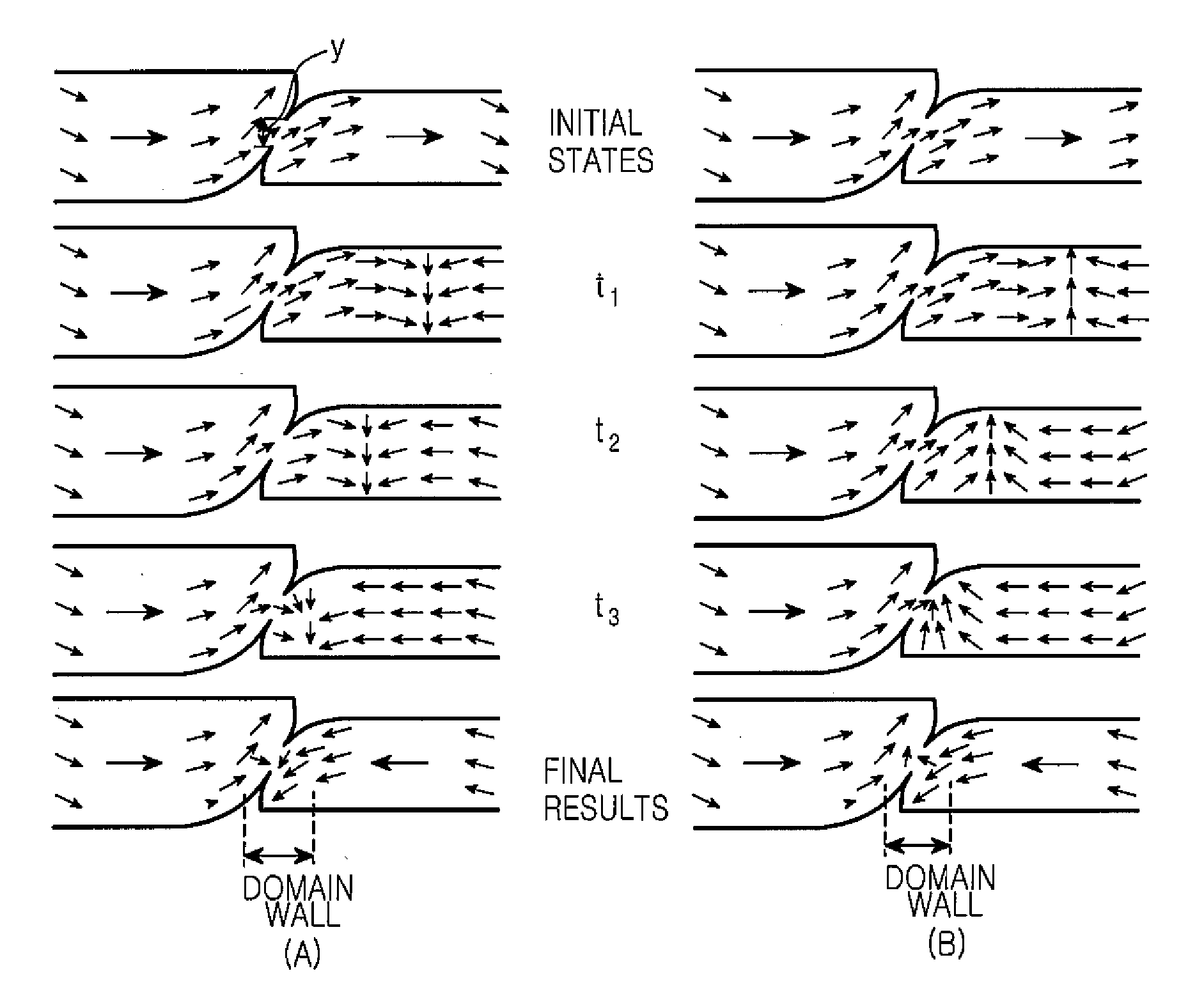
[0028] FIGS. 3(a) and 3(b) illustrate nanocontacts forming domain walls with equal thickness regardless of initial spin moment orientation of contact wire when a contact length is 0 nm in a nanocontact structure according to the present invention.

[0029] In the first contact wire, a contact plane including a contact area has a quadrant. The second contact wire contacts the first contact wire in a contact area and has a quadrant-shaped contact plane symmetrical with the quadrant contact plane of the first contact wire with respect to origin. Both ends of the quadrant are contacted with each other. The width of the first contact wire is 150 nm and the width of another contact wire is 125 nm.

[0030] A width y of the contact plane of both contact wires is 2-15 nm and a length x is 0 nm. In an initial state, the spin moment orientations of the contact wire are different. When a magnetic field of 100 Oe is applied to the right contact wire for t1 (300 pico seconds), a domain wall is formed...

second embodiment

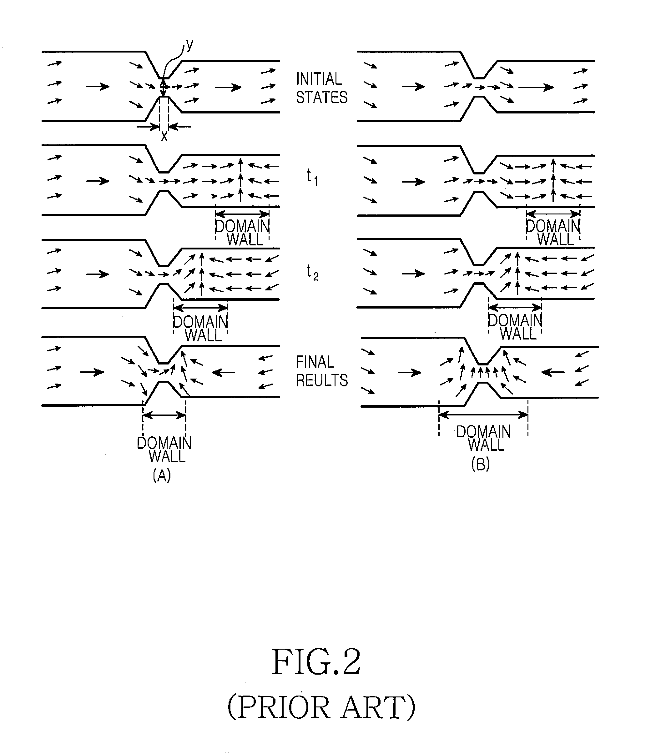
[0037] According to the nanocontact structure of the second embodiment, in the first contact wire, a contact plane including a contact area has a predetermined inclined shape. The second contact wire contacts the first contact wire in a contact area and has a contact plane forming an inclined angle symmetrical with the inclined angle of the first contact wire.

[0038] Although the use of NiFe (especially, Ni81Fe19) as the contact wire has been described above, materials (e.g., Co or Ni) in which there are more up spin than down spin in a Fermi energy, may also be used.

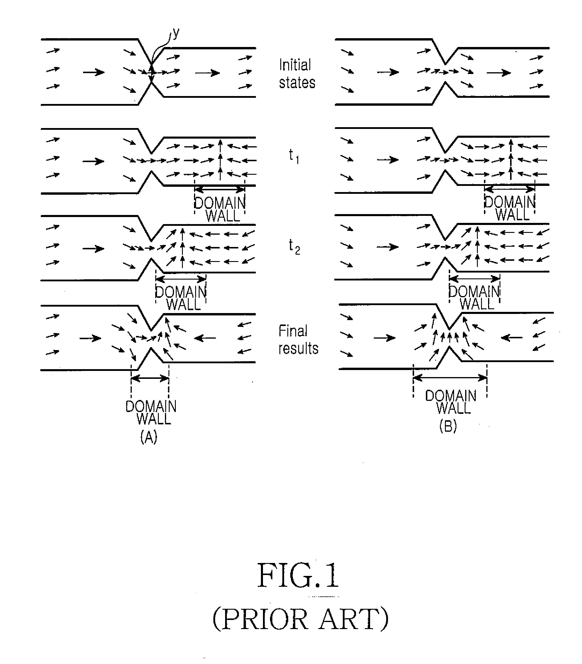
[0039] As described above, the contact area of two contact wires constituting the nanocontacts is formed in a quadrant shape symmetrical with origin. Thus, domain wall occurring when the magnetization directions of the first and second nanowires are opposite to each other by apply a magnetic field without regard to the initial spin moment orientation of the contact wire can have constant thickness. Consequently, it is p...


PUM

PropertyMeasurementUnit
widthaaaaaaaaaa
lengthaaaaaaaaaa
lengthaaaaaaaaaa

Abstract

A nanocontact between contact wires is provided. The contact plane of the first nanocontact wire has a quadrant shape. The contact plane of the second nanocontact wire contacting the first nanocontact wire has a quadrant shape symmetrical with the quadrant contact plane of the first nanocontact wire with respect to origin. Thus, magnetization directions of the first and second nanowires are opposite to each other, regardless of initial spin moment orientation of the nanowire. When domain wall is formed, the thickness of the domain wall becomes constant, such that ballistic magnetoresistance ratio can be constant and reproducible.

Description

PRIORITY [0001] This application claims priority under 35 U.S.C. §119 to an application entitled “Nanocontacts Having Improved Contact Shape” filed in the Korean Intellectual Property Office on Mar. 21, 2006 and allocated Serial No. 2006-25632, the contents of which are incorporated herein by reference. BACKGROUND OF THE INVENTION [0002] 1. Field of the Invention [0003] The present invention relates generally to a nanocontact, and in particular, to a nanocontact that constantly maintains ballistic magnetoresistance (BMR) by implementing domain wall with a constant thickness, regardless of initial spin moment orientation. [0004] 2. Description of the Related Art [0005] With the growth of mobile application markets, the demand for large-capacity nonvolatile memory and small-sized hard disc drive (HDD) is increasing. Ballistic magnetoresistance (BMR) devices are studied for the nonvolatile memory and HDD components. [0006] The ballistic magnetoresistance device can obtain very high mag...

Claims


Application Information

Patent Timeline
Patent Type & Authority Applications(United States)
IPC IPC(8): G11B5/127G11B5/33
CPCB82Y10/00G11B5/39G11C11/14G11C19/0808H01F41/34H01L43/08G11C11/54H10N50/10B82Y25/00
Inventor KIM, YOUNG KEUNKIM, SE-DONGCHUN, BYONG-SUN
Owner KOREA CHUNGANG EDUCATIONAL FOUND
Why Eureka
Try Eureka