Optical Device For A Display Having Tapered Waveguide And Process For Making The Same

Active Publication Date: 2007-09-27
SEKONIX
View PDF7 Cites 16 Cited by
  • Summary
  • Abstract
  • Description
  • Claims
  • Application Information

AI Technical Summary

Benefits of technology

[0061] As described above, the optical device according to the invention has an improved light efficiency, and thus can provide for a product having an excellent luminance, as compared with the conventional ones, when using an identical light source.
[0062] In addition, according to the invention, an optical device for a display having a stabilized light-absorbing region can be obtained.
[0063] Furthermore, the present invention provides a simplified process for fabricating such optical devices, thus improving production efficiency.
[0064] In the case where fine particles having magnetic property such as iron oxide is used as the light-absorbing particles, the fabrication process can be simplified. When the final product is used as a screen, th

Problems solved by technology

As such, the optical device of FIG. 2 requires numerous fine lenses on the surface thereof, which leads to a cumbersome manufacturing process.
In U.S. Pat. No. 5,462,700, the waveguide is formed using ultraviolet rays and thus usable medium is limited and the selection range for mediums having a lower refraction index is more narrowed.
Due to the trend of pursuing a large-scale screen, these patented inventions cause an increase in the number of process steps and the materials cost, and thus fail to meet the current or future requirements therefor.
Thus, a difference of about 0.3 in refraction indices between two mediums causes a difficulty and limitation in the design of a waveguide.
In case of such large-scale screens, provision of a metallic coating to the front face thereof causes many difficulties and problems, in terms of quality, productivity, facility or the like.
In particular, it is difficult to selectivel

Method used


Image

  • Optical Device For A Display Having Tapered Waveguide And Process For Making The Same
  • Optical Device For A Display Having Tapered Waveguide And Process For Making The Same
  • Optical Device For A Display Having Tapered Waveguide And Process For Making The Same

Examples


Example

[0082] The preferred embodiments of the present invention will be hereafter described in detail with reference to the accompanying drawings.

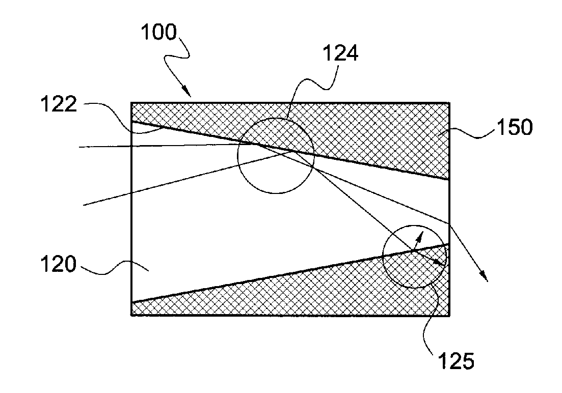
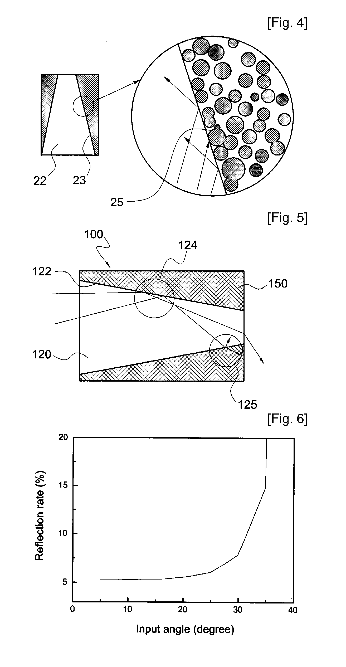
[0083] Referring to FIG. 5, imaging light rays are inputted into a waveguide 120 of an optical device for a display 100 and the input imaging light rays are reflected on the sidewall 122 of the waveguide 120. At this time, the imaging light rays are totally reflected on the sidewall 122 or passes through the sidewall 122, depending upon the input angle thereof. If the input angle of the imaging light rays is larger than the critical angle thereof (in case of light ray 124), the light rays are totally reflected or mostly reflected on the sidewall 122 of the waveguide 120. If the input angle of the imaging light rays is smaller than the critical angle thereof (in case of light ray 125), the imaging light rays are partially total-reflected, and partially pass through the waveguide 120 and absorbed in a light absorbing section 150, to thereby signi...


PUM


Abstract

Disclosed is an optical device for a display having a tapered waveguide and a method of fabricating such devices. In order to reduce light absorption inside the waveguide, a light-absorbing material is coated on the front surface only of the optical device Alternatively, a space adjacent to the waveguide is coated with a material having a refraction index different from the waveguide, preferably, lower than that of the waveguide and then filled with a light-absorbing material. In addition, a large- and uniform-sized light-absorbing material may be filled in the space. The optical device has an improved light efficiency, and thus exhibits an excellent luminance, as compared with the conventional ones, when using an identical light source. Furthermore, the fabrication method can produce such optical devices in a simplified manner, thus improving production efficiency.

Description

TECHNICAL FIELD [0001] The present invention relates to an optical device for a display and a method of fabricating the same. More particularly, the invention relates to an optical device for a display having a tapered waveguide and a method of fabricating such devices. BACKGROUND ART [0002] In general, an optical device for a display such as a projection TV, a screen for rear-projection projectors, a TFT-LCD, a PDT TV, or a CRT monitor has a fine lens structure or a waveguide structure in order to broaden the viewing angle thereof. The present invention relates to an optical device for a display having a waveguide structure and a method of manufacturing such devices. [0003] Conventional optical devices for displays will be explained in brief, referring to FIGS. 1 and 2. [0004]FIG. 1 is an enlarged view of the screen of a conventional optical device for a display. FIG. 2 is an enlarged sectional view of a conventional optical device for a display. [0005] As shown in FIGS. 1 and 2, t...

Claims


Application Information

Patent Timeline
IPC IPC(8): G02B6/02B05D5/06G02B6/06G02F1/1335
CPCG02B6/08G03B21/625G02F1/133524G02B6/10
Inventor HWANG, GYUHWANYU, YOUNGBINLEE, HYUNSOO
Owner SEKONIX
Why Eureka
Try Eureka