Semiconductor device and method for manufacturing the same

a technology of memory element and semiconductor device, which is applied in the direction of semiconductor device, basic electric element, electrical apparatus, etc., can solve the problems of unable to overcome the problem, unable to withstand voltage failure or the like of tunnel insulation film responsive to a high voltage, and impossible to overcome the problem

Inactive Publication Date: 2007-10-04
KK TOSHIBA
View PDF1 Cites 20 Cited by
  • Summary
  • Abstract
  • Description
  • Claims
  • Application Information

AI Technical Summary

Benefits of technology

[0011]According to an aspect of the invention, there is provided a semiconductor device comprising: a semiconductor substrate; a tunnel insulation film provided on the surface of the semiconductor substrate, charge trap states at which an electron potential energy is higher than a Fermi level of the semiconductor substrate being p

Problems solved by technology

However, as downsizing of the memory cell or the like advances, a withstand voltage failure or the like of the tunnel insulation film responsive to a high voltage is more likely to occur.
Specifically,

Method used


Image

  • Semiconductor device and method for manufacturing the same
  • Semiconductor device and method for manufacturing the same
  • Semiconductor device and method for manufacturing the same

Examples


first embodiment

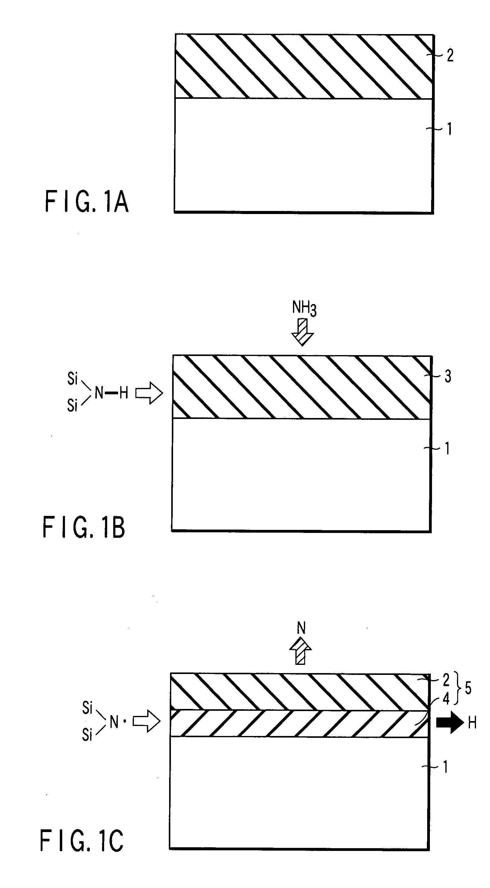
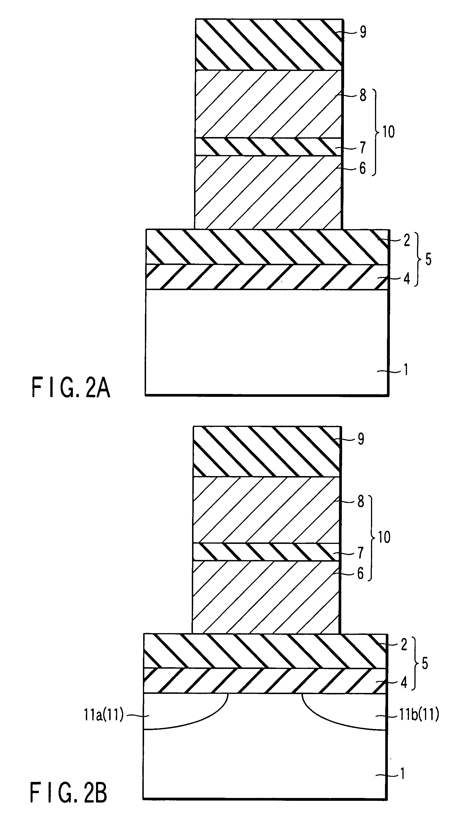
[0031]First, a first embodiment of the present invention will be described with reference to FIGS. 1A to 7C. FIGS. 1A to 2B are process cross sections showing a method for manufacturing a semiconductor device according to the first embodiment. FIG. 3 is a plan view showing a memory element forming region of the semiconductor device according to the first embodiment as seen from above thereof. FIG. 4 a sectional view taken along the cutting line A-A1 shown in FIG. 3. FIG. 5 is a sectional view taken along the cutting line B-B′ shown in FIG. 3. FIGS. 6A and 6B are views schematically showing an energy band diagram of a tunnel insulation film of the semiconductor device according to the first embodiment. FIGS. 7A to 7C are views schematically showing an energy level and a presence range in a film thickness direction, of the tunnel insulation film possessed by the semiconductor device according to the first embodiment.

[0032]In the present embodiment, of memory type semiconductor devices...

second embodiment

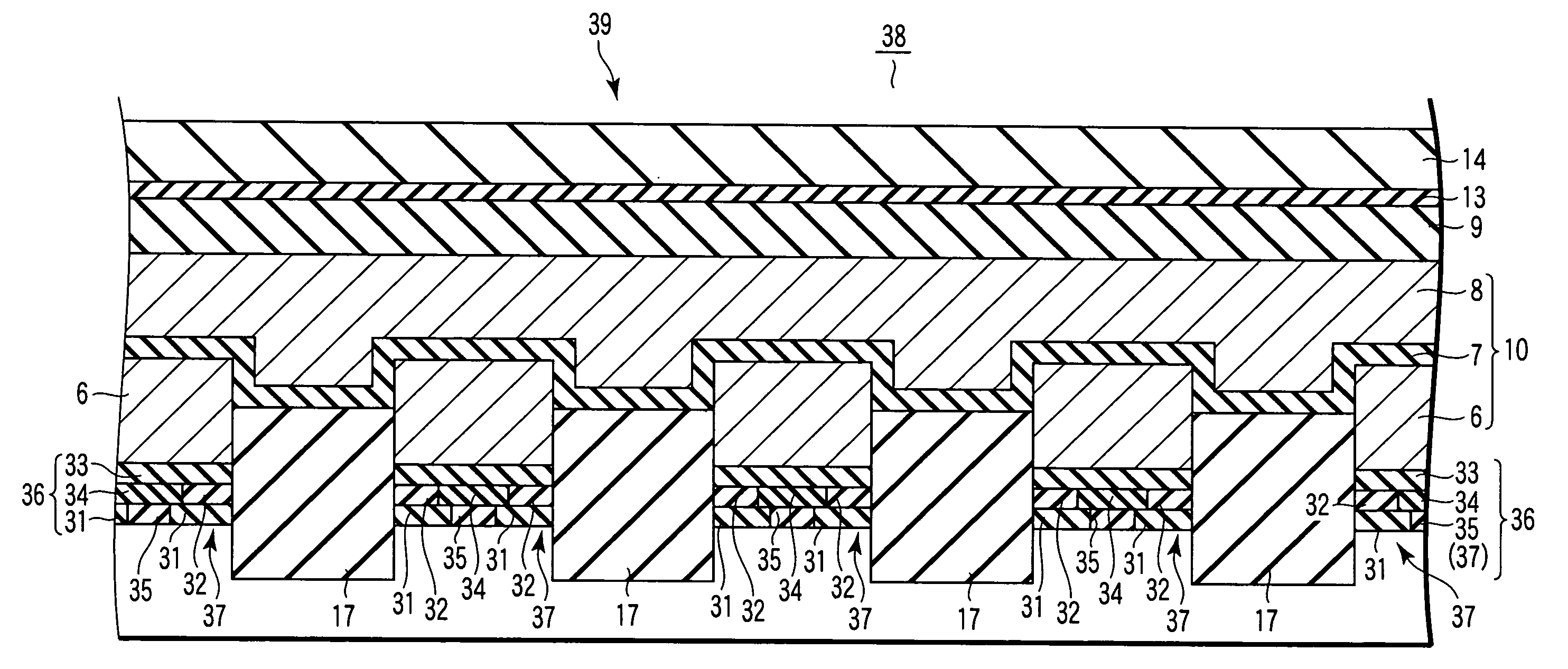
[0066]Now, a second embodiment according to the invention will be described with reference to FIGS. 8A to 14. FIGS. 8A to 10 are process sectional sections showing a method for manufacturing a semiconductor device according to the second embodiment. FIG. 11 is a plan view showing a memory element forming region of the semiconductor device according to the invention as seen from above thereof. FIG. 12 is a sectional view taken along the cutting line C-C′ shown in FIG. 11. FIG. 13 is a sectional view taken along the line D-D′ shown in FIG. 11. FIG. 14A is a sectional view showing a spatial distribution of charge trap states of a tunnel insulation film possessed by the semiconductor device according to the second embodiment. FIG. 14B is a sectional view showing a spatial distribution of charge trap states of a tunnel insulation film possessed by a semiconductor device according to an example of a modified second embodiment. Like constituent elements shown in the first embodiment descri...


PUM


Abstract

A semiconductor device including a semiconductor substrate, a tunnel insulation film provided on the surface of the semiconductor substrate, charge trap states at which an electron potential energy is higher than a Fermi level of the semiconductor substrate being provided at part of the tunnel insulation film at least in the vicinity of an interface with the semiconductor substrate, and at least one charge storage layer being provided on the tunnel insulation film, charges supplied from the semiconductor substrate via the tunnel insulation film being accumulated in the charge storage layer.

Description

CROSS-REFERENCE TO RELATED APPLICATIONS[0001]This application is based upon and claims the benefit of priority from prior Japanese Patent Applications No. 2006-097538, filed Mar. 31, 2006; and No. 2006-299202, filed Nov. 2, 2006, the entire contents of both of which are incorporated herein by reference.BACKGROUND OF THE INVENTION[0002]1. Field of the Invention[0003]The present invention relates to a semiconductor apparatus equipped with a memory element and a method for manufacturing the same. In particular, the present invention relates to a semiconductor device equipped with a memory element having its improved electrical characteristics and a method for manufacturing the same.[0004]2. Description of the Related Art[0005]Among semiconductor devices, there is a memory type semiconductor device called a flash memory. As described in Jpn. Pat. Appln. KOKAI Publication No. 2002-261097, a memory element (memory cell) in a flash memory generally has a structure described below.[0006]A s...

Claims


Application Information

Patent Timeline
IPC IPC(8): H01L29/76
CPCH01L27/115H01L29/7883H01L29/42332H01L27/11568H10B43/30H10B69/00
Inventor OZAWA, YOSHIO
Owner KK TOSHIBA
Why Eureka
Try Eureka