Carbon nanotube via interconnect

Active Publication Date: 2007-10-04
DELPHI TECH IP LTD
View PDF12 Cites 72 Cited by
  • Summary
  • Abstract
  • Description
  • Claims
  • Application Information

AI Technical Summary

Benefits of technology

[0006] In an aspect of this invention, there is provided a technique of electrically interconnecting circuit components using carbon nanotubes as electrical conductors. The carbon nanotube interconnects may be used for electrically connecting an integrated circuit device, such as a flip chip, to another integrated circuit device (die stacking), or to a substrate, such as a printed circuit board or other package carrie

Problems solved by technology

As is well known to those who design integrated circuits or use integrated circuits in the design of various electronic packages, the performance characteristics of electronic devices operating in the microwave frequency range are highly susceptible to deleterious effects caused by stray capacitances and inductances that can be generated at wire bonds of the type that have been

Method used


Image

  • Carbon nanotube via interconnect
  • Carbon nanotube via interconnect
  • Carbon nanotube via interconnect

Examples


Example

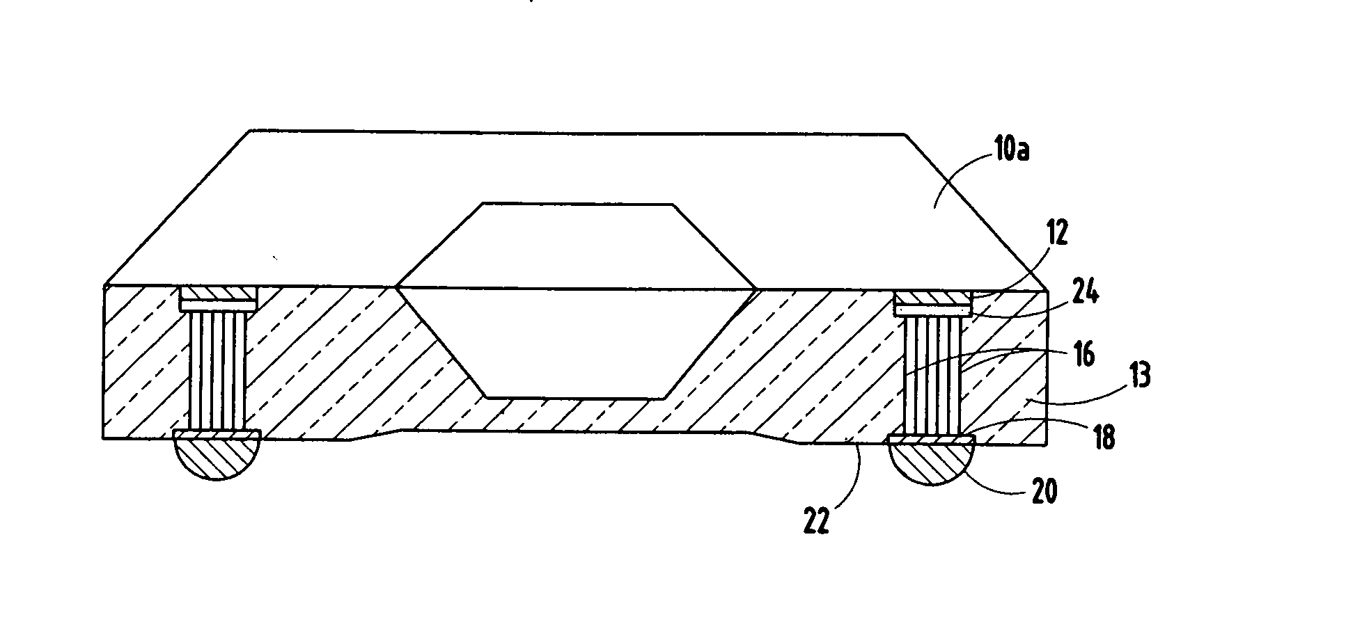
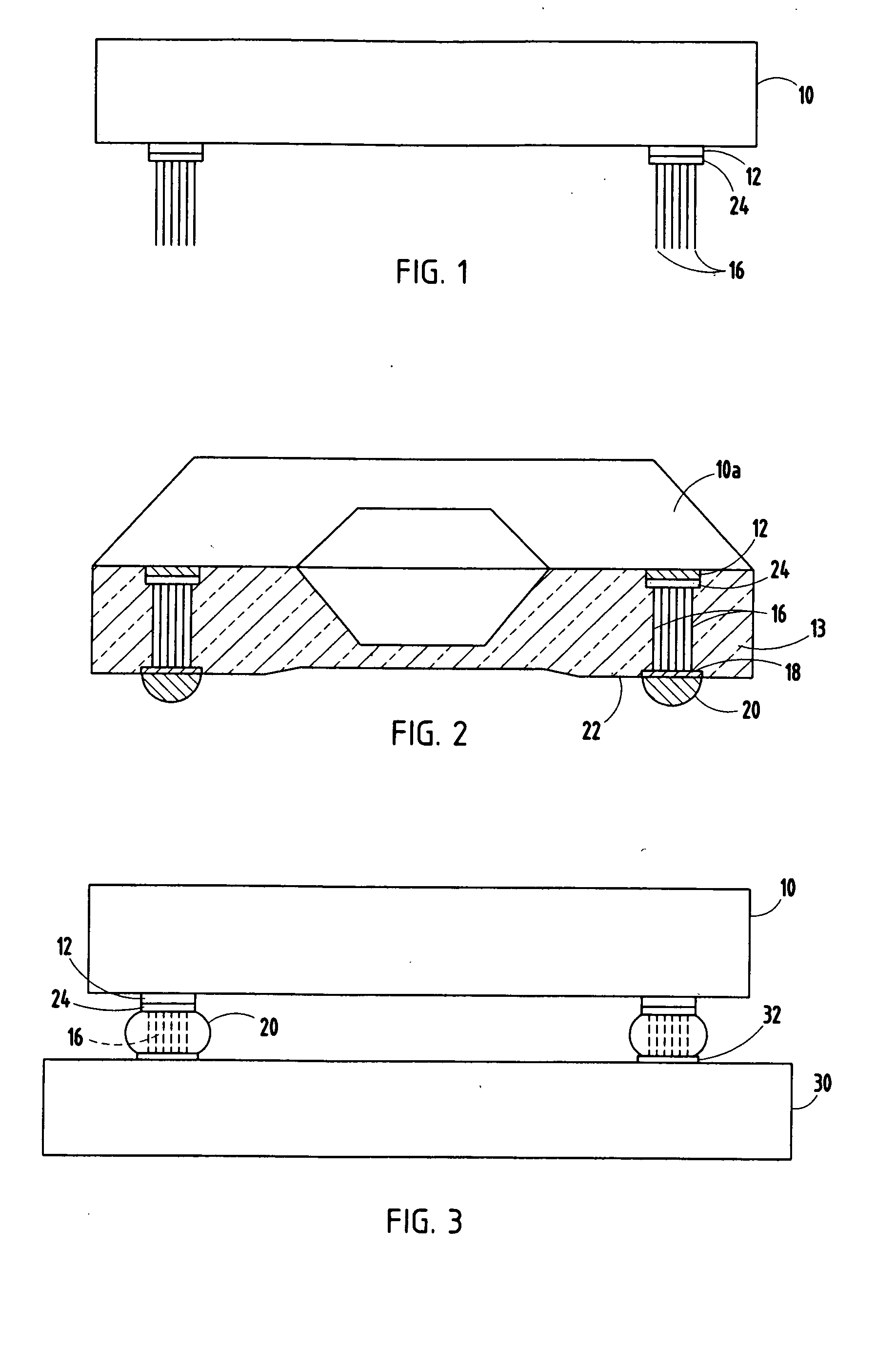
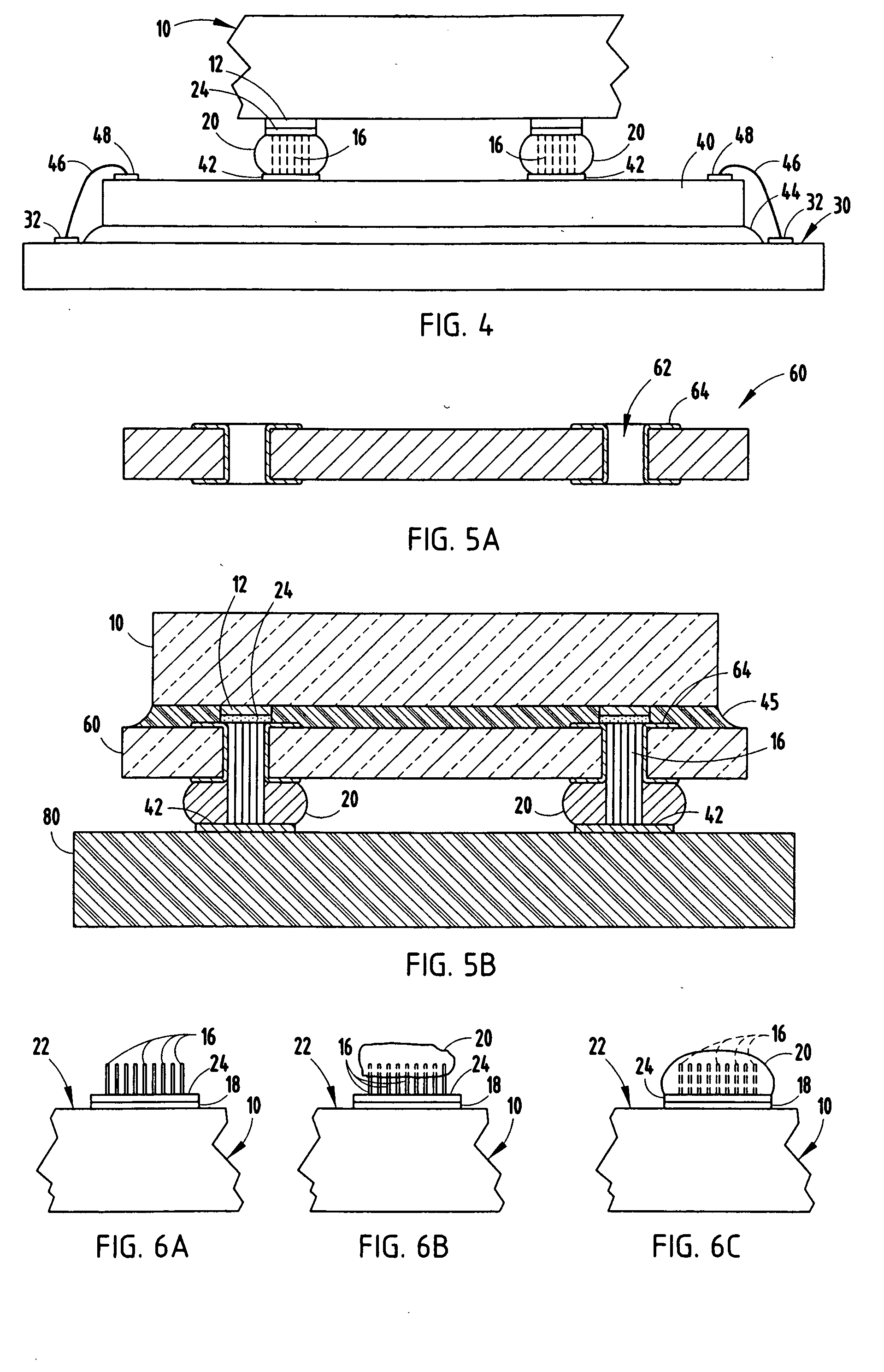
[0017] In FIG. 1, there is shown an integrated circuit device 10. Device 10 includes an electrically conductive input / output (I / O) pad 12 (e.g., aluminium, copper, etc.) on which a catalyst layer 24 is deposited. Suitable catalysts for growing carbon nanotubes, and techniques for depositing catalyst layer 24 are well known. Device 10 has a carbon nanotube via interconnect comprising at least one carbon nanotube 16 directly grown on I / O pads 12 of IC device 10. Normally numerous carbon nanotubes are grown on each pad. A solder bead optionally deposited on a metal terminal to complete a flip chip device in which a reflow technique may be used for electrically and mechanically connecting integrated circuit device 10 to another device or to a substrate or package carrier such as a printed circuit board. CNT growth is done at wafer level. After wafer sawing, individual IC or MEMS / NEMS device may be flip chip mounted on a substrate or second device, using flux (with optional pre-formed so...


PUM


Abstract

An electronic device that facilitates improved electrical and thermal performance and/or allows fabrication of smaller electronic devices exhibiting excellent performance characteristics, especially for devices operating at microwave frequencies, includes an input/output pad, and a carbon nanotube extending from the input/output pad to provide wafer-level nano-interconnect for flip chip interconnections and die stacking on a substrate.

Description

TECHNICAL FIELD [0001] This invention relates to integrated circuitry, and more particularly to improved via interconnects at wafer-level for electrically connecting surface mount integrated circuits to other devices or to a substrate, such as a printed circuit board or other package carrier. BACKGROUND OF THE INVENTION [0002] There is a constant demand for electronic devices having smaller features that are more densely crowded together on a single substrate or chip. At the same time, consumers of such devices are demanding faster operating speeds and higher reliability, such as are achieved with monolithic microwave integrated circuits (MMICs). Monolithic microwave integrated circuits are formed of a plurality of devices or circuit components that are fabricated on a single semiconductor substrate, and are designed to operate at microwave frequencies, which are generally regarded to be between about 3,000 and 300,000 microns, corresponding to operating frequencies of from about 1 ...

Claims


Application Information

Patent Timeline
IPC IPC(8): H01J63/04
CPCB81C1/00095H01L2224/16235H01L23/49827H01L23/49877H01L24/11H01L24/12H01L24/16H01L24/81H01L24/94H01L2224/0231H01L2224/13099H01L2224/274H01L2224/81136H01L2224/8121H01L2224/81815H01L2924/01013H01L2924/01022H01L2924/01027H01L2924/01029H01L2924/01047H01L2924/01074H01L2924/01075H01L2924/01078H01L2924/01079H01L2924/01082H01L2924/09701H01L2924/14H01L2924/1423H01L2924/30105H01L2924/30107H05K3/3436H05K3/4007H05K2201/026H01L2924/01006H01L2924/01024H01L2924/01033H01L2924/01076H01L2924/014H01L2224/0401B82Y10/00H01L2224/05124H01L2224/05147H01L2224/05655H01L2224/05193H01L2224/13193H01L2224/131H01L2224/13076H01L24/13H01L24/05H01L24/03Y02P70/50H01L2924/00014
Inventor TEO, KIAT CHOONWONG, WAI KWANPAN, BINGHUA
Owner DELPHI TECH IP LTD
Why Eureka
Try Eureka