Image sensor

a technology of image sensor and processing circuit, which is applied in the direction of picture signal generator, solid-state device signal generator, television system, etc., can solve the problem of putting a load on the processing circuit process, and achieve the effect of reducing load and increasing readout speed

Active Publication Date: 2007-10-04
CANON KK
View PDF21 Cites 32 Cited by
  • Summary
  • Abstract
  • Description
  • Claims
  • Application Information

AI Technical Summary

Benefits of technology

[0010]It is an object of the present invention to increase the readout speed in the low resolution readout mode, or in addition to this, reduce the load on a processing circuit which processes pixel signals read out in the low resolution readout mode.
[0024]According to another aspect of the present invention, the load on a processing circuit which processes pixel signals read out in the low resolution readout mode can be reduced.

Problems solved by technology

However, Japanese Patent Laid-Open No. 2005-286933 does not describe any idea of increasing the frame rate in capturing a moving image from that in capturing a still image.
However, Japanese Patent Laid-Open No. 2005-130382 does not describe any concept of parallely outputting sums through a plurality of channels.
However, this puts a load on the process of a processing circuit which processes the pixel signals.

Method used


Image

  • Image sensor
  • Image sensor
  • Image sensor

Examples


first embodiment

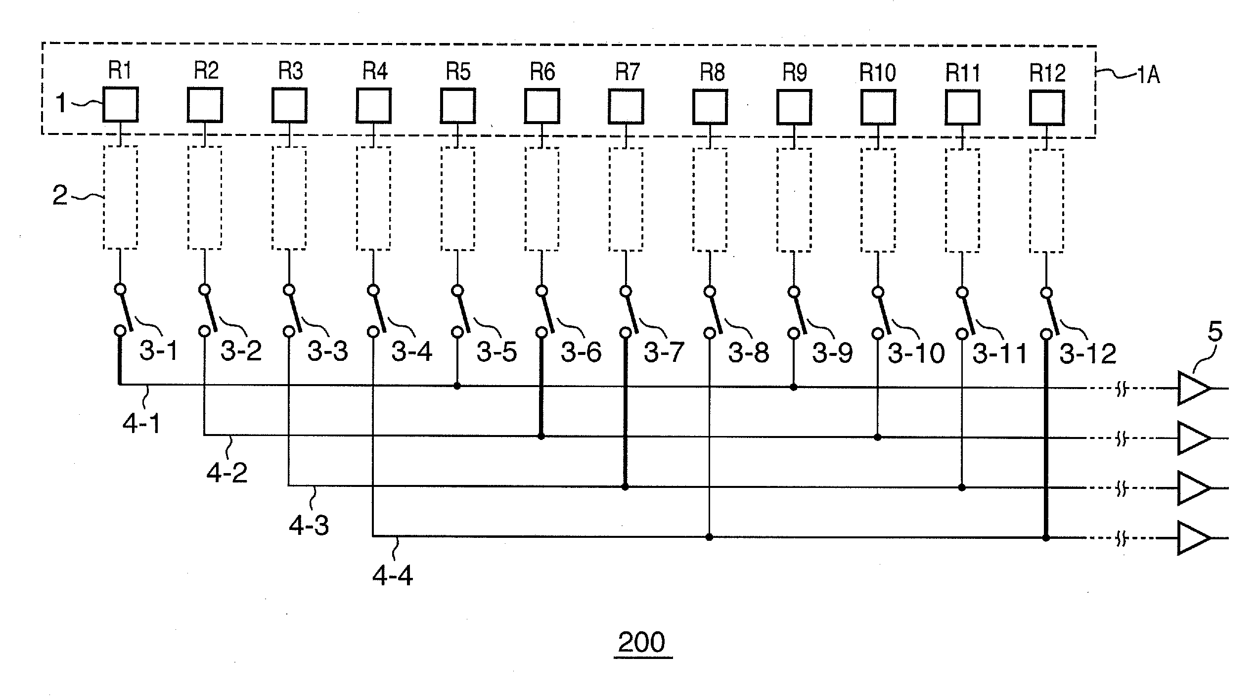
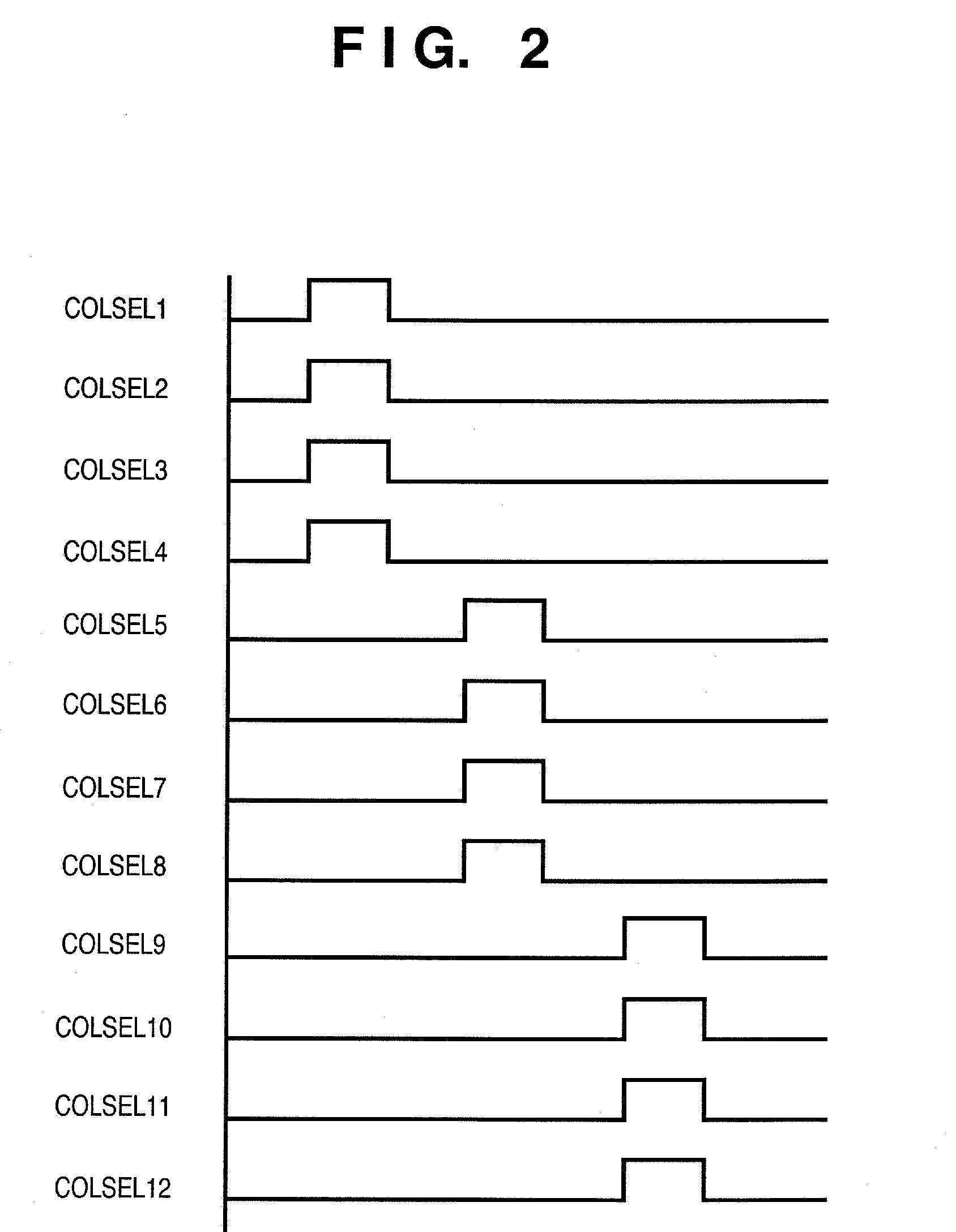
[0047]FIG. 1 is a circuit diagram showing the schematic arrangement of an image sensor according to the first embodiment of the present invention. An image sensor 200 comprises a pixel array area 1A where a plurality of pixels 1 are arrayed. In the pixel array area 1A, the pixels 1 can be arranged to form a plurality of columns or one or a plurality of rows. FIG. 1 shows only pixels R1 to R12 of one row corresponding to a red filter. Each readout circuit 2 generates a pixel signal based on a signal supplied from a corresponding pixel. The readout circuit 2 supplies a pixel signal to the input terminal of a corresponding column selecting switch 3. The readout circuit 2 may incorporate an amplifier circuit and the like, or may be formed from only a conductive line for transmitting a pixel signal. The output terminals of the column selecting switches 3, i.e., 3-1, 3-2, 3-3, 3-4, . . . connect to horizontal output lines (output channels) 4, i.e., 4-1, 4-2, 4-3, and 4-4. The first embodi...

second embodiment

[0063]FIG. 4 is a circuit diagram showing the schematic arrangement of an image sensor according to the second embodiment of the present invention. The arrangement shown in FIG. 4 is different from that shown in FIG. 1 in that averaging circuits 6 are inserted between readout circuits 2 and column selecting switches 3. The averaging circuit 6 averages signals in a target readout area in the low resolution readout mode.

[0064]The averaging circuit (operation circuit) 6 calculates and outputs the average value of pixel signals in accordance with an activation signal. An output from each averaging circuit 6 is supplied to one of four horizontal output lines through one of the column selecting switches 3 corresponding to three pixels subjected to averaging. Outputs from the averaging circuits 6 can be supplied to horizontal output lines 4-1, 4-2, 4-3, and 4-4 through the switches 3-1, 3-6, 3-7, and 3-12, similar to the thinning readout mode in the first embodiment.

[0065]According to the ...

third embodiment

[0076]FIG. 8 is a circuit diagram showing the schematic arrangement of an image sensor according to the third embodiment of the present invention. The arrangement shown in FIG. 8 is different from that shown in FIG. 4 in that add circuits 10 are inserted between readout circuits 2 and column selecting switches 3, instead of the averaging circuits 6.

[0077]The add circuit (operation circuit) 10 calculates and outputs the sum of pixel signals in accordance with an activation signal. An output from each add circuit 10 is supplied to one of four horizontal output lines through one of the switches corresponding to three pixels subjected to addition. Similar to the first and second embodiments, sum pixel signals from respective target readout areas are output to horizontal output lines 4-1, 4-2, 4-3, and 4-4 using the switches 3-1, 3-6, 3-7, and 3-12.

[0078]According to the third embodiment, similar to the first embodiment, the image sensor can parallely output a plurality of pixel signals ...


PUM


Abstract

An image sensor has a plurality of pixels arrayed to form a plurality of columns. The sensor includes a plurality of readout circuits which generate pixel signals based on signals supplied from the pixels of respective columns, a plurality of output channels, a plurality of column selecting switches, and a control circuit which controls the plurality of column selecting switches. The control circuit controls the plurality of column selecting switches so as to output the pixel signals of target readout pixels to output channels selected based on a selection rule in the spatial order of the pixels in the full pixel readout mode. The control circuit controls the plurality of column selecting switches so as to output the thinned-out pixel signals of target readout areas to output channels selected based on the same rule as the selection rule in the spatial order of the areas in the thinning readout mode.

Description

BACKGROUND OF THE INVENTION[0001]1. Field of the Invention[0002]The present invention relates to an image sensor and, more particularly, to an image sensor having a plurality of output channels.[0003]2. Description of the Related Art[0004]These days, image sensors for digital cameras make remarkable progress and are rapidly gaining a larger number of pixels for higher resolution of still images. Along with this, it is an urgent issue to increase the pixel signal readout speed in order to ensure sequential shooting performance necessary for a camera. Japanese Patent Laid-Open No. 2005-286933 discloses a CCD image sensor which parallely reads out pixel signals through a plurality of column shift registers to increase the readout speed.[0005]A digital camera can capture still images and even moving images. The digital camera generally uses one image sensor to capture both still and moving images. The image sensor requires high resolution for still images, and requires high frame rate f...

Claims


Application Information

Patent Timeline
Patent Type & Authority Applications(United States)
IPC IPC(8): H04N5/335H04N5/341H04N5/345H04N5/369H04N5/376H04N5/378
CPCH04N5/3456H04N9/045H04N5/378H04N5/347H04N25/445H04N25/46H04N25/75
Inventor HIYAMA, HIROKIHATANO, YUICHIROARISHIMA, YU
Owner CANON KK
Why Eureka
Try Eureka