Solid-state image sensing device and method of operating the same

Inactive Publication Date: 2007-10-04
RENESAS ELECTRONICS CORP
View PDF4 Cites 3 Cited by
  • Summary
  • Abstract
  • Description
  • Claims
  • Application Information

AI Technical Summary

Benefits of technology

[0020]Such architecture allows a trailing edge of the clock signals fed to the output region is sharper than a trailing edge of the clock signals fed to the main CCD region.
[0021]In another embodiment, the clock signals fed to the third and fourth transfer electrodes have symmetric waveforms with respect to the voltage, resulting in that the duration of the pull-up of the clock signal fed to the third transfer electrode is identical to the pull-down of the clock sign

Problems solved by technology

Additionally, the conventional CCD 100 may suffer from coupling noise on the output thereof. FIG. 6 is a timing chart illustrating the waveforms of the clock signals and the output voltage.
This undesirably causes coupling noise applied to the floating diffusion 105 from the output stage electrode pair 113 fed with the third clock signal Φ

Method used


Image

  • Solid-state image sensing device and method of operating the same
  • Solid-state image sensing device and method of operating the same
  • Solid-state image sensing device and method of operating the same

Examples


Example

First Embodiment

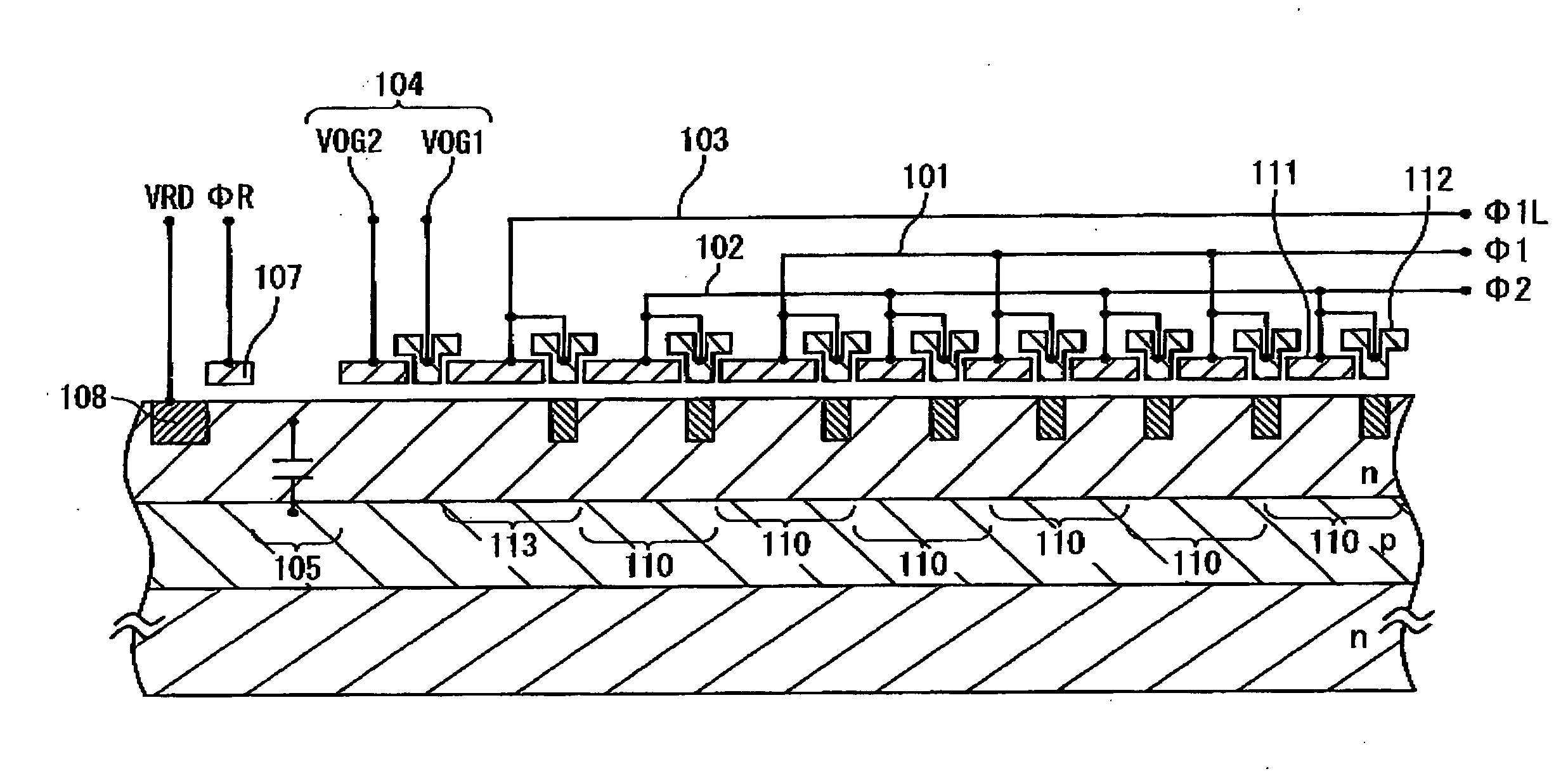
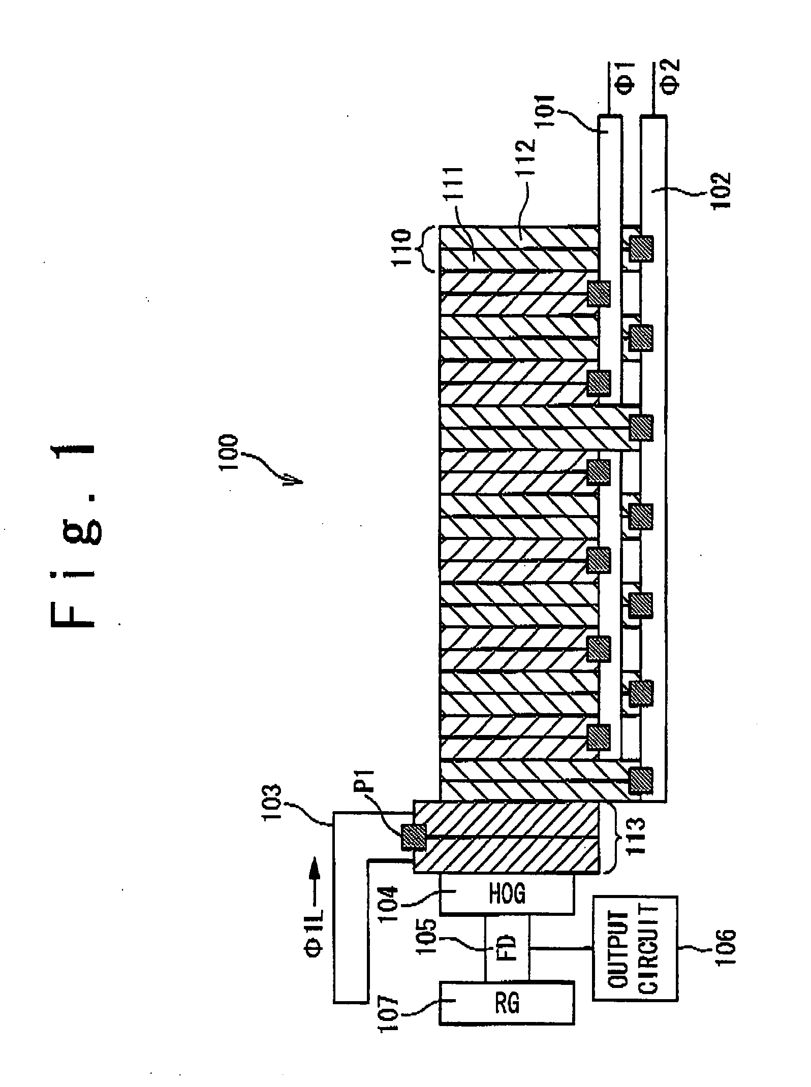
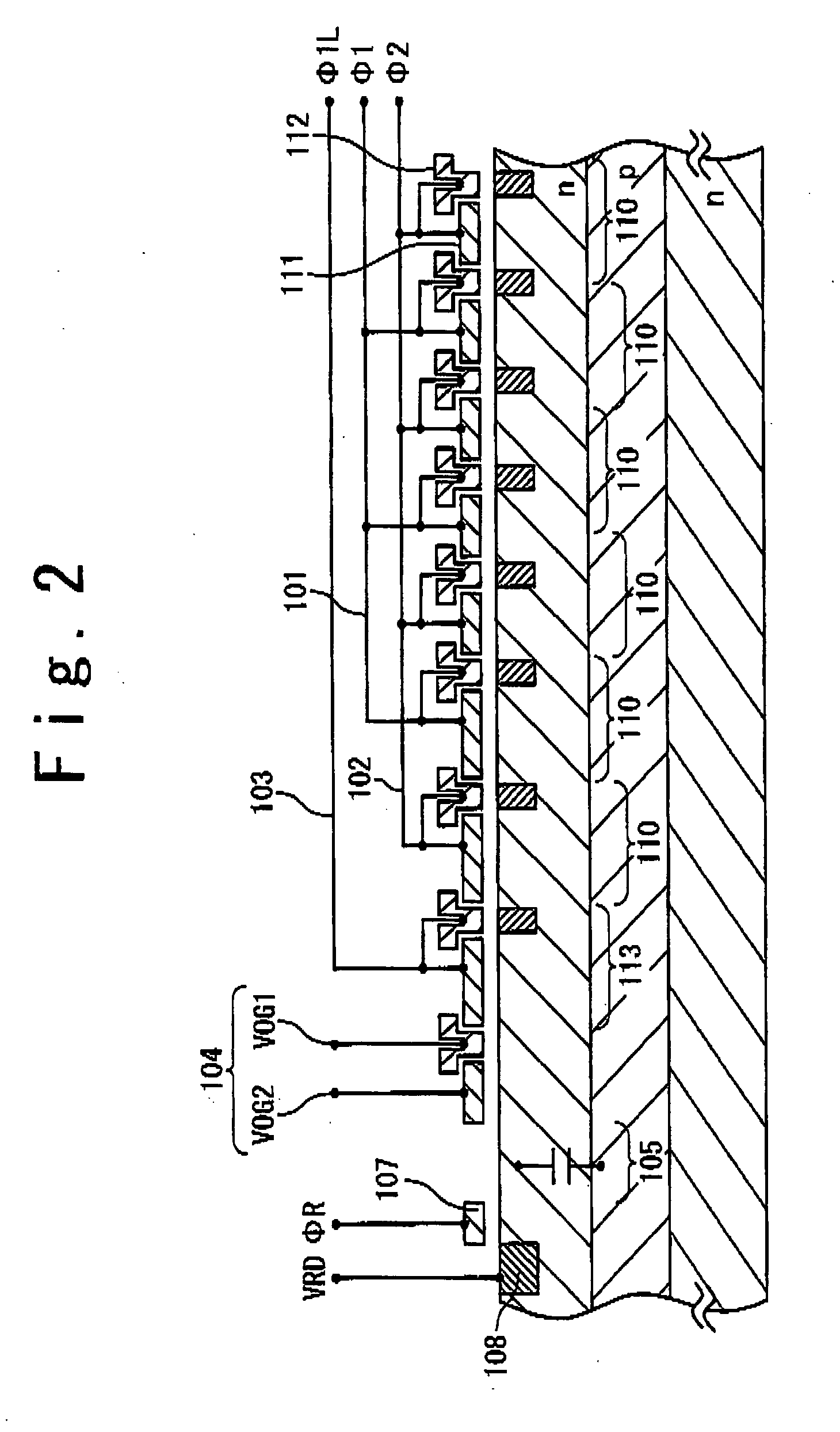
[0049]FIG. 7 is a plan view illustrating the structure of a solid-state image sensing device in a first embodiment of the present invention. The solid-state image sensing device in the first embodiment is provided with a CCD (charge coupling device) 1 for transferring electric charges, and a clock generator 2 feeding a set of clock signals to the CCD 1. The CCD 1 includes first transfer electrode pairs 4, second transfer electrode pairs 3, third transfer electrode pairs 6, fourth transfer electrode pairs 5, an output gate 7, a floating diode 9, a reset gate 10, and a reset drain 11. The first transfer electrode pairs 4 commonly receive a first clock signal Φ1, and the second transfer electrode pairs 3 commonly receive a second clock signal Φ2. The third transfer electrode pairs 6 commonly receive a third clock signal Φ1L, and the fourth transfer electrode pairs 5 commonly receive a second clock signal Φ2L. The first and third clock signals Φ1 and Φ1L have the same ph...

Example

Second Embodiment

[0083]In the following, a description is given of a second embodiment of the present invention. In the following, same elements are denoted by same numerals as in the first embodiment; elements denoted by the same numeral are identically designed to provide the same function. Therefore, duplicated descriptions are not given for the elements denoted by the same numeral in the first embodiment.

[0084]FIG. 16 is a plan view of the solid-state image sensing device in the second embodiment. The solid-state image sensing device in the second embodiment is provided with the CCD 1 and the clock generator 2. The CCD 1 additionally includes a fifth transfer electrode pair 6a. The solid-state image sensing device in the second embodiment achieves summing signal charges of two adjacent pixels through appropriately controlling the waveform of the fifth clock signal Φ1L′. The clock generator circuit 23 within the clock generator 2 generators the fifth clock signal Φ1L′ in addition...

Example

Third Embodiment

[0093]FIG. 22 is a plan view illustrating the third embodiment of the present invention. The clock generator 2 in the third embodiment includes a set of inverters 22-1 to 22-4. The inputs of the first and third inverters 22-1 and 22-3 are commonly connected with a first node N1 that is connected with a first output of the clock generator circuit 23. The inputs of the second and fourth inverters 22-2 and 22-4 are commonly connected with a second node N2 that is connected with a second output of the clock generator circuit 23, Such arrangement of the clock generator 2 effectively reduces the number of the outputs of the clock generator circuit 23.


PUM


Abstract

A charge coupled device is provided with; an output gate; a main CCD region operated in response to a set of clock signals; and an output region positioned between the output gate and the main CCD region and designed to transfer electric charges received from the main CCD region to the output gate. The main CCD region includes first and second transfer electrodes. The output region includes third and fourth transfer electrodes receiving clock signals which are phase-reversed from each other. The set of clock signals received by the main CCD region and the clock signals received by the output region are outputted from different driver circuits.

Description

BACKGROUND OF THE INVENTION[0001]1. Field of the Invention[0002]The present invention relates to a solid-state image sensing device, more particularly, to a solid-state image sensing device that incorporates a CCD (charge coupled device).[0003]2. Description of the Related Art[0004]The advance of the semiconductor technology enhances the use of solid-state image sensing devices, which receive light on the light receiving surface from a target body through an optical system typically including a lens and so forth, and photoelectrically convert the intensity of the received light into the corresponding amounts of electric charges to thereby generate electrical signals. A commercially-used solid-state image sensing device usually includes a CCD (charge coupled device). The advance in the fine processing technology of the semiconductor device allows manufacturing a solid-state image sensing device with an increased pixel density, that is, with an improved fineness.[0005]When the solid-s...

Claims


Application Information

Patent Timeline
IPC IPC(8): H04N5/335H01L27/148H04N5/341H04N5/357H04N5/372H04N5/376
CPCH04N5/335H01L27/14843H04N25/00
Inventor MATSUYAMA, EIJI
Owner RENESAS ELECTRONICS CORP
Why Eureka
Try Eureka