FFS mode liquid crystal display panel

Active Publication Date: 2007-10-04
JAPAN DISPLAY WEST
View PDF8 Cites 59 Cited by
  • Summary
  • Abstract
  • Description
  • Claims
  • Application Information

AI Technical Summary

Benefits of technology

[0024]By providing the features stated above, the present invention offers beneficial advantages as described below. With the above FFS mode LCD panel, while switching elements, such as TFTs to operate the pixel electrodes are positioned differently depending on whether they are in odd-numbered or even-numbered rows, the length of the signal lines can be shortened. Further, the slits provided at the pixel electrodes of each pixel are symmetric with respect to an axis parallel to the scanning lines, while keeping dead space at a minimum. Furthermore, the slits are symmetric by each row with respect to another axis perpendicular to the scanning lines. This makes it possible to maintain symmetrical viewing angle in both directions parallel and perpendicular to the scanning lines, utilizing a display opening. Also, no spots are generated in a transverse direction as in the related art, and an FFS mode LCD panel with a bright display can be obtained.
[0025]Furthermore, as the slits of the pixel electrodes provided at both sides of the axis parallel to the scanning lin

Problems solved by technology

But, because the common electrode 55 is formed of the same metal material as the common line 53, there are problems of a low aperture ratio and a low transmittance, and color changes depending on viewing angle.
As they cannot form into the same shape, a

Method used


Image

  • FFS mode liquid crystal display panel
  • FFS mode liquid crystal display panel
  • FFS mode liquid crystal display panel

Examples


Example

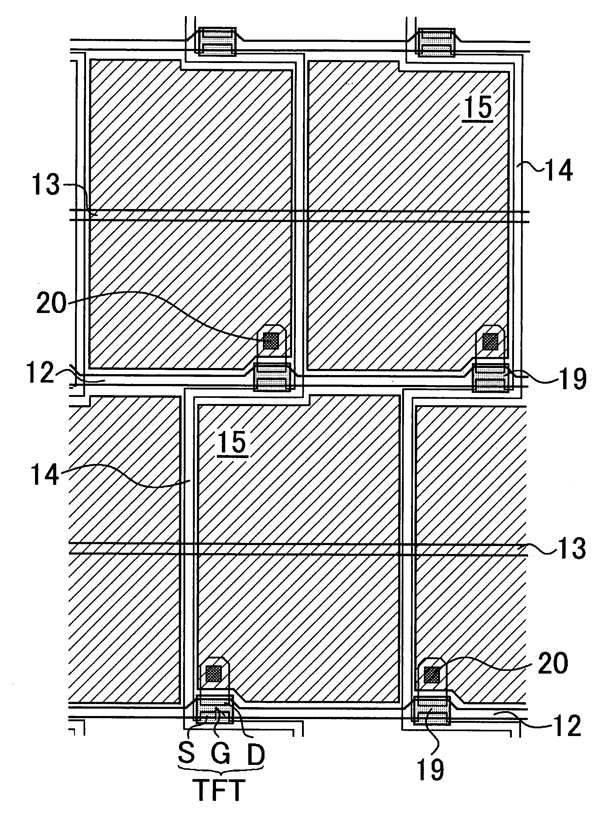
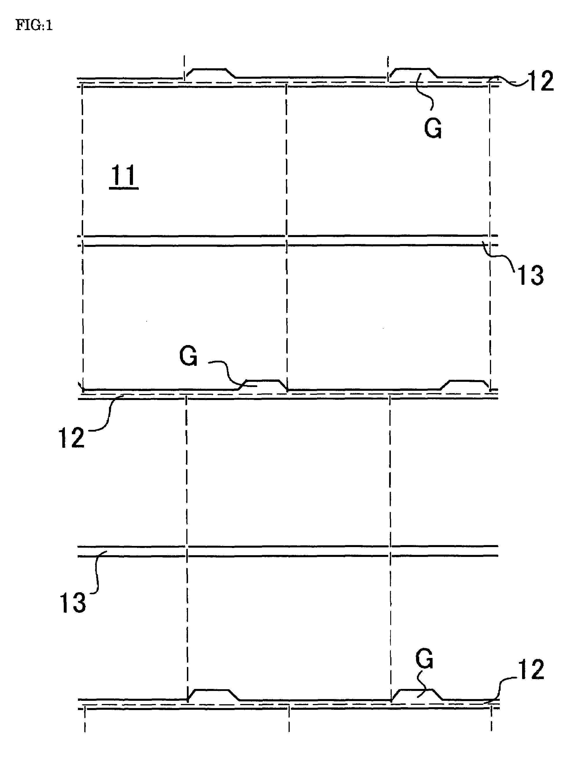
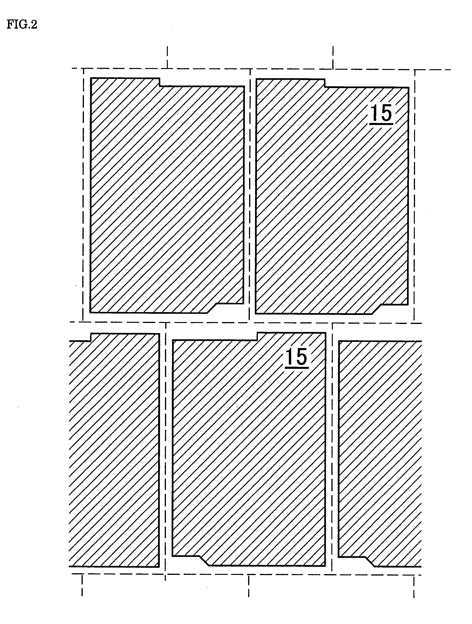
[0045]Hereinafter, preferred embodiments of the present invention will be described with reference to the drawings. The following embodiments are examples to show features of an FFS mode LCD panel, in order of manufacturing steps, to embody the concept of the present invention. The present invention is not intended to be specified to this FFS mode LCD panel, and may be equally applied to other embodiments not departing from the spirit and scope of the appended claims.

[0046]FIG. 1 is a diagram showing a pattern of scanning lines and common lines formed by a scanning line and common line forming process. FIG. 2 is a diagram showing a pattern of common electrodes formed by a common electrode forming process. FIG. 3 is a diagram showing a pattern of semiconductor layers formed by a semiconductor forming process. FIG. 4 is a diagram showing a pattern of signal lines and drain electrodes formed by a signal line and drain electrode forming process. FIG. 5 is a diagram showing a pattern of ...


PUM


Abstract

The present invention provides a fringe field switching (FFS) mode liquid crystal display panel including a plurality of scanning lines 12 and common lines 13 provided in parallel, a plurality of signal lines 14 provided in a crank manner in a direction perpendicular to the scanning lines 12, and pixel electrodes 181 and 182 each formed between the plurality of scanning lines 12 and signal lines 14 in a delta arrangement. Each of the pixel electrodes 181 and 182 has a plurality of slits 171 and 172, respectively, inclined in different directions to each other with respect to an axis x parallel to the scanning lines 12 and positioned between adjacent scanning lines 12. The pixel electrodes 181 in odd-numbered rows and the pixel electrodes 182 in even-numbered rows are inverted to each other with respect to another axis perpendicular to the axis x. With such features, the FFS mode liquid crystal display panel provides symmetrical viewing angle generating no spots in a transverse direction, a wide viewing angle, a bright display with high transmittance and excellent display quality.

Description

BACKGROUND[0001]1. Technical Field[0002]The present invention relates to a fringe field switching (hereinafter, referred to as “FFS”) mode liquid crystal display (LCD) panel. More particularly, the present invention relates to an FFS mode LCD panel in a dual-domain structure in which pixels are arranged in a delta arrangement.[0003]2. Related Art[0004]In recent years, LCD panels are widely used not only for information and communication devices but also for electrical devices in general. Typical LCD panels include one pair of substrates made of glass and the like formed with electrodes and the like on their surfaces, and a liquid crystal layer formed between the pair of substrates. By applying a voltage to the electrodes on both substrates to change transmittance of light by rearranging liquid crystal molecules, various images are displayed. This is a so-called longitudinal electric field mode. There are a twisted nematic (TN) mode and a vertical alignment (VA) mode in a longitudina...

Claims


Application Information

Patent Timeline
IPC IPC(8): G02F1/1343
CPCG02F1/133707G02F1/134363G02F2201/40G02F2201/128G02F2001/134372G02F1/134372G02F1/133G02F1/1343
Inventor KANEKO, HIDEKIHORIGUCHI, MASAHIRO
Owner JAPAN DISPLAY WEST
Why Eureka
Try Eureka