Semiconductor integrated circuit device, charge pump circuit, and electric appliance

a technology of integrated circuit devices and semiconductors, applied in the direction of power conversion systems, dc-dc conversion, instruments, etc., can solve problems such as reducing production efficiency

Inactive Publication Date: 2007-10-11
ROHM CO LTD
View PDF2 Cites 8 Cited by
  • Summary
  • Abstract
  • Description
  • Claims
  • Application Information

AI Technical Summary

Benefits of technology

[0013]In view of the conventionally experienced problems described above, an object of the present invention is to provide versatile semiconductor integrated circuit devices that can be used to form charge pump circuits having different step-up factors, and to provide charge pump circuits and electric appliances provided with such semiconductor integrated circuit devices.

Problems solved by technology

This undesirably results in reduced production efficiency.

Method used


Image

  • Semiconductor integrated circuit device, charge pump circuit, and electric appliance
  • Semiconductor integrated circuit device, charge pump circuit, and electric appliance
  • Semiconductor integrated circuit device, charge pump circuit, and electric appliance

Examples


Embodiment Construction

[0025]Hereinafter, the present invention will be described by way of an example in which it is applied to a versatile semiconductor integrated circuit device that can be used to form two- to sevenfold step-up charge pump circuits.

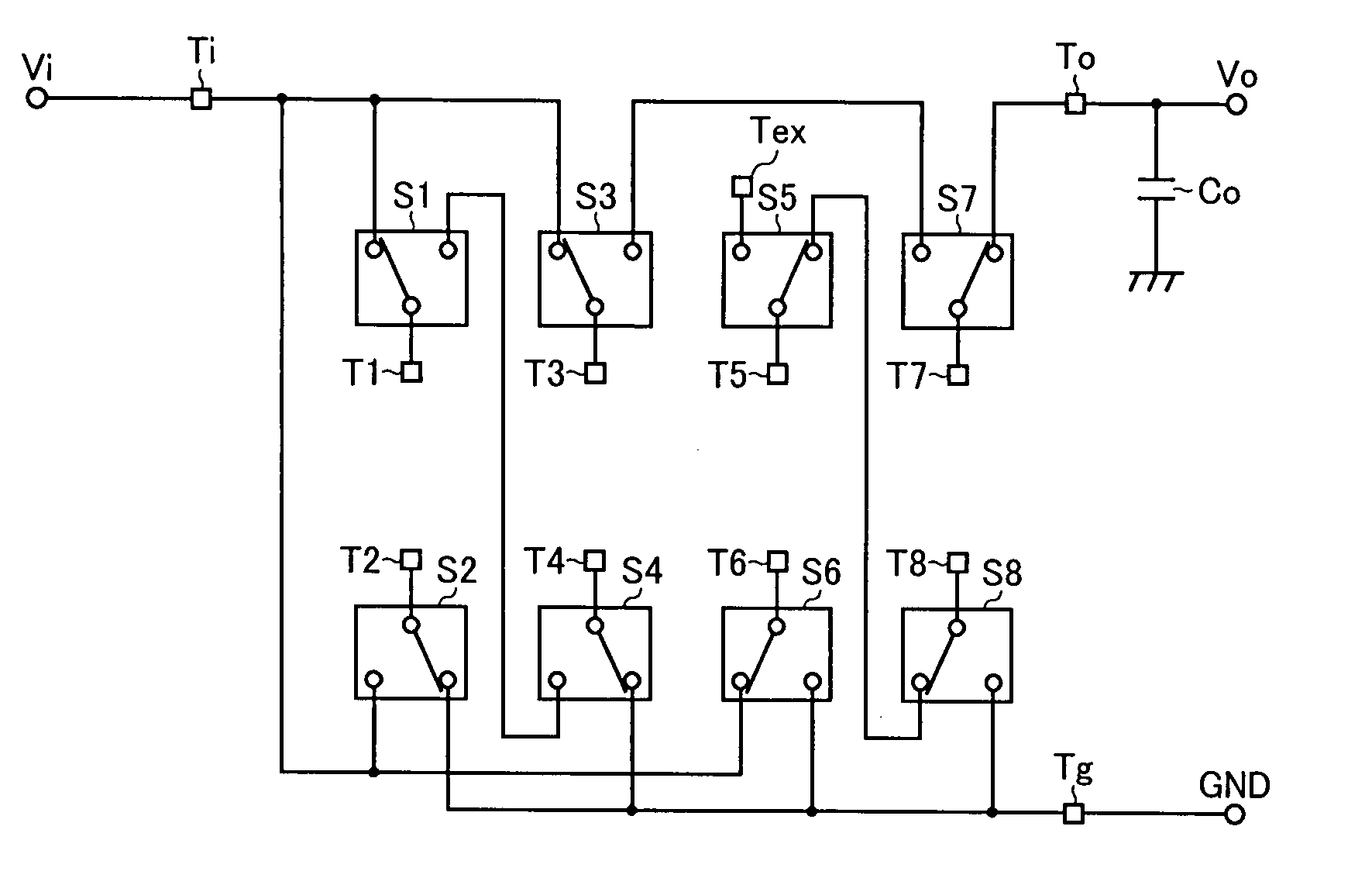
[0026]FIG. 1 is a diagram showing an embodiment of a semiconductor integrated circuit device according to the invention.

[0027]As shown in FIG. 1, in addition to an input terminal Ti to which an input voltage Vi is applied, an output terminal To from which an output voltage Vo is outputted, a ground terminal Tg to which a ground voltage GND is applied, external terminals T1 to T8 to which a charge transfer capacitor (not shown in this figure) is externally fitted, and charge transfer switches S1 to S8 that are provided one for each of the external terminals T1 to T8 and are each formed as a MOSFET or a bipolar transistor, the semiconductor integrated circuit device includes a step-up factor switching terminal Tex that can change the terminal to which it is c...


PUM


Abstract

In addition to an input terminal, an output terminal, a ground terminal, a plurality of external terminals, and a plurality of charge transfer switches, a semiconductor integrated circuit device has a step-up factor switching terminal. Here, the plurality of charge transfer switches each have a common contact connected to corresponding one of the plurality of external terminals and two selection contacts alternatively connected to the common contact, and one of the selection contacts of the plurality of charge transfer switches is connected to the step-up factor switching terminal, and each of the other selection contacts is connected to one of the input terminal, the output terminal, the ground terminal, and the rest of the other selection contacts. With this configuration, it is possible to make the semiconductor integrated circuit device versatile so that it can be used to form charge pump circuits having different step-up factors.

Description

[0001]This application is based on Japanese Patent Application No. 2006-077964 filed on Mar. 22, 2006, the contents of which are hereby incorporated by reference.BACKGROUND OF THE INVENTION[0002]1. Field of the Invention[0003]The present invention relates to semiconductor integrated circuit devices for use in charge pump circuits, and more particularly to a step-up factor changing technique adopted thereby.[0004]2. Description of Related Art[0005]FIG. 9 is a circuit diagram showing an example of a conventional charge pump circuit. A charge pump circuit 100 shown in this figure produces, from an input voltage Vi, a desired output voltage Vo (=2Vi) by turning a plurality of charge transfer switches 101 to 104 ON / OFF at regular intervals according to a clock signal (not shown) in such a way as to charge and discharge a charge transfer capacitor 105.[0006]The above-described positive stepping-up will be specifically described. The output voltage Vo is produced as follows. First, during ...

Claims


Application Information

Patent Timeline
Patent Type & Authority Applications(United States)
IPC IPC(8): H02M3/18H02M7/00
CPCH02M3/07
Inventor IMANAKA, YOSHINORI
Owner ROHM CO LTD
Why Eureka
Try Eureka